Note
The version of ESP-IDF corresponding to this document is v5.5.0
I2C Basic Example
Note
This document is automatically translated using AI. Please excuse any detailed errors. The official English version is still in progress.
Example Description
This example demonstrates how to initialize and configure the I2C interface, as well as how to communicate with the MPU9250 sensor via the I2C master, including reading data from the slave register and releasing related resources after completion.
How to Run
The complete code for the example can be found at I2C Basic Master Example. Instructions for configuration before running, corresponding GPIO pins, build and flash process can be found in the README.md file in the example directory.
For custom configuration items and default values, refer to the Macro Definition Description section.
Header File Description
The header files used in this example cover basic modules such as FreeRTOS task management, log output, I2C driver, and system configuration. They provide support for I2C initialization, data reading, and resource release.
The header files are categorized by function as follows:
FreeRTOS Task Scheduling : Provides task creation and scheduling functions.
#include "freertos/FreeRTOS.h"
#include "freertos/task.h"
System Tools : Provides input and output, system configuration, and log output functions.
#include <stdio.h>
#include "sdkconfig.h"
#include "esp_log.h"
I2C Driver : Provides initialization, read and write operations, and resource release functions in I2C master mode.
#include "driver/i2c_master.h"
Macro Definition Description
The macro definitions involved in this example are mainly used to configure the pins, port number, working frequency, and timeout of the I2C master, and also define the slave address and key register address of the MPU9250 sensor.
The macro definitions are categorized by function as follows:
I2C Master Configuration
Use configuration macros to define the GPIO pin numbers used by the I2C clock line (SCL) and data line (SDA). In the example, the clock line corresponds to GPIO 4; the data line corresponds to GPIO 5.
#define I2C_MASTER_SCL_IO           CONFIG_I2C_MASTER_SCL
#define I2C_MASTER_SDA_IO           CONFIG_I2C_MASTER_SDA
Define the port number used by I2C, this example uses
I2C_NUM_0.#define I2C_MASTER_NUM I2C_NUM_0
Use configuration macros to define the clock frequency of the I2C master. In the example, the clock frequency is 400000 Hz.
#define I2C_MASTER_FREQ_HZ CONFIG_I2C_MASTER_FREQUENCY
Define the send buffer and receive buffer in master mode. Both are disabled (set to 0) in this example because the I2C master does not need to use internal buffers.
#define I2C_MASTER_TX_BUF_DISABLE   0
#define I2C_MASTER_RX_BUF_DISABLE   0
Define the timeout period, used to limit the waiting time in I2C read and write operations, to avoid bus blocking, in milliseconds.
#define I2C_MASTER_TIMEOUT_MS 1000
Note
Configuration macros start with
CONFIG_, which are automatically generated by the ESP-IDF build system based on themenuconfigsettings and saved in thesdkconfigfile.When defining GPIO pins, use configuration macros instead of directly writing pin numbers. This allows for flexible modification of pins at compile time without modifying the source code, facilitating project expansion and management.
If you want to change the pins used, just modify
menuconfigand rebuild/compile the example, and it will automatically update without manually changing the code.Disabling send and receive buffers helps save resources and is suitable for general host communication scenarios.
MPU9250 Sensor Configuration :
Define the slave address of the MPU9250 device and the key register addresses for subsequent register read and write operations.
#define MPU9250_SENSOR_ADDR         0x68
#define MPU9250_WHO_AM_I_REG_ADDR   0x75
#define MPU9250_PWR_MGMT_1_REG_ADDR 0x6B
#define MPU9250_RESET_BIT           7
Note
The slave device address and register address are determined by the specific I2C slave model, not user-defined. If you are using other I2C slaves, you need to refer to the target device manual to modify the corresponding macro definitions.
The
WHO_AM_Iregister is used to read the sensor chip ID to verify whether the device is properly connected.The
PWR_MGMT_1register is used for power management, and the reset operation can be completed by setting the 7th bit (RESET_BIT).
Task Function Description
This example includes three core functions to implement communication between the I2C host and the MPU9250 sensor: the I2C host initialization function, the register read function, and the register write function.
I2C Host Initialization Function
i2c_master_init() is used to initialize the I2C host and bind the target device.
This initialization step is universal and applicable to all scenarios involving I2C peripherals. You only need to modify the port number, slave address, and related configuration parameters according to the specific device. For a detailed explanation of the steps and the involved structure members, refer to the I2C Initialization section.
Input Parameter |
Parameter Function |
Parameter Description |
|---|---|---|
|
I2C bus handle pointer |
The valid handle returned after the bus is successfully created, used for subsequent read and write operations on this bus. |
|
I2C device handle pointer |
The valid device handle returned after adding the device to the I2C bus, used for subsequent communication with this device. |
Register Write and Read Function
mpu9250_register_read() is used to read the contents of the MPU6050 register address.
Input Parameter |
Parameter Function |
Parameter Description |
|---|---|---|
|
I2C device handle |
The valid device handle returned after adding the device to the I2C bus, used to specify the target slave device. |
|
Target register address |
The register address of the target device to be read. |
|
Data buffer pointer |
Used to store data read from the register. After calling the function, data is written to this memory area. |
|
Read byte length |
Specifies the number of bytes to read from the register, and the buffer size must be sufficient to hold the data. |
This function calls i2c_master_transmit_receive() to implement register write and read, with the following execution logic:
Send the target register address as write data to MPU9250 to specify the register and verify the device connection. The slave should acknowledge the successful reception.
The slave sends the register content, the master acknowledges the reception, and reads the specified length of data.
The master stores the received data in the
databuffer.
For more explanations and the principle of the function, refer to I2C Master Write then Read. The parameter description of i2c_master_transmit_receive() can be found in I2C Interface.
Register Write Function
mpu9250_register_write_byte() is used to write a single byte of data to the specified register of MPU9250.
Input Parameter |
Parameter Function |
Parameter Description |
|---|---|---|
|
I2C device handle |
The valid device handle returned after adding the device to the I2C bus, used to specify the target slave device. |
|
Target register address |
The address of the target device register to be read. |
|
Data to be written |
Single byte data. |
The function execution logic is as follows:
Combine the register address and the data to be written into the write buffer
write_buf[].Call
i2c_master_transmit()to write the buffer data to the specified register of the slave device, achieving register write.
For more explanations and the principle of the function, refer to I2C Master Write. The parameter description of i2c_master_transmit() can be found in I2C Interface.
Main Function Description
This example demonstrates the initialization of the I2C master, communication with the MPU9250 sensor, and resource release.
Define variables:
Define the array
data[]to store the data read from MPU9250.Define the bus handle
bus_handleand device handledev_handlefor subsequent saving of the returned handles.
Call
i2c_master_init()to initialize the I2C bus and add the slave device, completing the connection between the master and the slave. After successful execution, it returns the corresponding handle and prints a log to indicate that I2C initialization is complete.Call
mpu9250_register_read()to read the content in theWHO_AM_Iregister.Call
mpu9250_register_write_byte()to set theRESET_BITof thePWR_MGMT_1register to 1, achieving the reset of MPU9250.
Call
i2c_master_bus_rm_device()to remove the slave device. For parameter description, refer to I2C Interface.Call
i2c_del_master_bus()to delete the I2C bus. For parameter description, refer to I2C Interface.
Note
Initialization and resource release are common processes for I2C, ensuring the bus and devices are correctly configured and released to avoid resource leaks.
Performing read and write operations are application-specific tasks, and register operations can be modified according to the actual functions of the slave device.
Program Phenomenon
In this example, the program controls read and write operations by sending register addresses to the slave device. The read operation uses a write register address and read data transaction, and the write operation uses a write register address and write data transaction. The corresponding timing diagram is as follows:
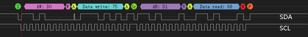
According to the timing diagram, the program execution can be summarized into the following stages:
Start Condition: Represented as
Sin the timing diagram, the master sends the start condition, marking the beginning of an I2C transaction. SDA is pulled low from high, while SCL remains high.Master Address Write: Represented as
AW : D0 Win the timing diagram, the master sends a 7-bit slave address plus a 1-bit write flag (W) to the slave on the rising edge of SCL. SDA outputs the address and write flag, and each bit of data is sampled by the slave when SCL is high.Slave Acknowledge: Represented as
Ain the timing diagram, the slave pulls SDA low to send ACK after receiving the address and recognizing it as a write operation.Master Data Write: Represented as
Data write: 75in the timing diagram, the master sends register data to the slave. SDA outputs the data, and each bit of data is sampled corresponding to the high level of SCL.Slave Acknowledge: Represented as
Ain the timing diagram, the slave pulls SDA low to send ACK after receiving the data.Repeated Start Condition: Represented as
Srin the timing diagram, the master sends the repeated start condition, preparing for the read operation. SDA is pulled low from high, while SCL remains high.Master Address Read: Represented as
AR : D1 Rin the timing diagram, the master sends a 7-bit slave address plus a 1-bit read flag (R) to the slave on the rising edge of SCL. SDA outputs the address and read flag, and each bit of data is sampled by the slave when SCL is high.Slave Data Read: Represented as
Read write: 68in the timing diagram, the slave outputs the register data to SDA, and the master samples the data on the rising edge of SCL.Master Acknowledge: Represented as
Nin the timing diagram, the master pulls SDA high to send NACK after receiving the last byte, indicating the end of this read operation.Stop Condition: Represented as
Pin the timing diagram, the master sends the stop condition, ending this I2C transaction. SDA is pulled high from low, while SCL remains high.