ESP-Mosaico V1.2
Older version: ESP-Mosaico V1.0
Note
This document covers CoreBoard V1.2 hardware. Please check the silkscreen version on the mainboard to confirm your board revision. See Hardware Revision Details for differences from V1.0.
The camera module is supported in the left slot only (H2). Do not insert it into the right slot. For installation and usage instructions, see the Camera Module User Guide.
This guide helps you get started with ESP-Mosaico and provides detailed information about the board.
ESP-Mosaico is an expandable smart interaction development kit based on ESP32-S31. It targets magnetic expansion toys, motion sensing, square touch display HMI, and edge voice/multimedia applications. The device integrates a 480 × 480 QSPI square touch display, ES8311 audio codec, NS4150B amplifier, BMI270 6-axis IMU, dual BMM150 magnetometers, SPI NAND flash, and left/right 2 × 10P, 2.54 mm pitch module headers.
The main controller is Espressif ESP32-S31, supporting 2.4 GHz Wi-Fi 6 (IEEE 802.11b/g/n/ax), Bluetooth® 5.4 (LE + BR/EDR), and IEEE 802.15.4 (Thread / Zigbee). For storage, the board provides 16 MB in-package PSRAM, onboard 16 MB SPI NOR flash, and onboard 1 Gbit SPI NAND flash for graphics, multimedia, and asset caching. The display uses a CO5300-driven 480 × 480 QSPI square touch display with a CST9220-series touch controller.
For audio, ESP-Mosaico integrates ES8311 and NS4150B Class-D PA. The power system supports USB Type-C 5 V and a 3.7 V / 65 mAh Li-ion battery, with TP4057 charging, BQ27220 fuel gauge, and SAM8108 power-switch control. Both the Type-C port and the left/right module interfaces support power input and output. A USB 2.0 High-Speed OTG port supports power, debug, and communication, and the board also reserves UART expansion capability and left/right module interfaces.
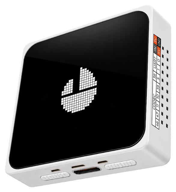
ESP-Mosaico Appearance (Click to enlarge)
The document consists of the following major sections:
Getting Started: Overview of the board and hardware/software setup instructions.
Hardware Reference: More detailed information about the board hardware.
Hardware Revision Details: Hardware revision history and known issues (if any).
Related Documents: Links to related documentation.
Disclaimer and Copyright Notice: Link to the disclaimer and copyright notice.
Getting Started
This section briefly introduces ESP-Mosaico and describes how to flash firmware and prepare the board.
Description of Components
ESP-Mosaico consists of a CoreBoard and a BaseBoard. The front views and their main components are shown first, followed by the back views and their main components.
Front
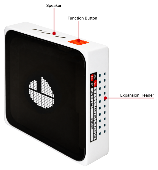
ESP-Mosaico Front (Click to enlarge)
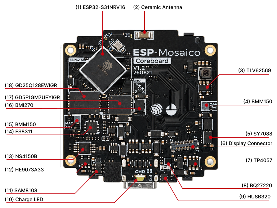
ESP-Mosaico CoreBoard Front (Click to enlarge)
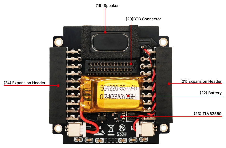
ESP-Mosaico BaseBoard Front (Click to enlarge)
The following describes the main components on the front PCB in clockwise order.
No. |
Key Component |
Description |
|---|---|---|
CoreBoard |
Core board integrating the SoC, RF antenna, power management, display connector, audio codec, and sensors. |
|
1 |
ESP32-S31NRV16 |
ESP32-S31 SoC, RISC-V 32-bit dual-core up to 320 MHz with 16 MB in-package PSRAM; supports 2.4 GHz Wi-Fi 6, Bluetooth 5.4 (LE + BR/EDR), and IEEE 802.15.4. |
2 |
KH-3216-A35 Ceramic Antenna |
2.4 GHz chip ceramic antenna for Wi-Fi and Bluetooth RF. |
3 |
TLV62569 |
Buck (DCDC) converter that converts the input supply to the system 3.3 V rail for the display. |
4 |
BMM150 |
3-axis magnetometer (BMM150 #2), I2C address 0x11. |
5 |
SY7088 |
Boost (BOOST) converter for rails higher than the battery voltage. |
6 |
Display Connector |
Connects the 480 × 480, 2.16-inch QSPI touch display (CO5300 driver + CST9220 touch). |
7 |
TP4057 |
Li-ion battery charger for the onboard battery. |
8 |
BQ27220 |
Fuel gauge at I2C address 0x55 for voltage, current, state of charge (SOC), and related status. |
9 |
HUSB320 |
USB Type-C interface controller that handles CC detection and controls the USB power direction. |
10 |
Charge LED |
Charge status indicator: orange while charging, white when fully charged. |
11 |
SAM8108 |
Power on/off controller used with the POWER button. |
12 |
HE9073A33 |
LDO providing a dedicated supply to the audio codec to reduce noise. |
13 |
NS4150B |
Low-EMI, filterless 3 W mono Class-D amplifier for the speaker. |
14 |
ES8311 |
Low-power mono audio codec, I2C address 0x19, connected to the SoC over I2S. |
15 |
BMM150 |
3-axis magnetometer (BMM150 #3), I2C address 0x12. |
16 |
BMI270 |
6-axis IMU (accelerometer + gyroscope), I2C address 0x69. |
17 |
GD5F1GM7UEYIGR |
1 Gbit (128 MB) SPI NAND flash for large-capacity asset storage. |
18 |
GD25Q128EWIGR |
16 MB (128 Mbit) SPI NOR flash for program and data storage. |
BaseBoard |
Base board integrating the speaker, battery, external 3.3 V buck, and left/right 2 × 10P module headers, mated to the CoreBoard through a board-to-board connector. |
|
19 |
Speaker |
Onboard speaker driven by the NS4150B amplifier. |
20 |
BTB Connector |
60-pin 0.5 mm board-to-board connector linking the CoreBoard and BaseBoard. |
21 |
Expansion Header |
2 × 10P dual-row, 2.54 mm pitch header on the right side of the figure, exposing GPIOs and power for expansion. |
22 |
Battery |
3.7 V / 65 mAh Li-ion battery for portable power. |
23 |
TLV62569 |
Buck (DCDC) converter that generates the external 3.3 V rail, isolated from the internal MCU supply. |
24 |
Expansion Header |
The other header, on the left side of the figure, exposing the remaining GPIOs and power. |
Back
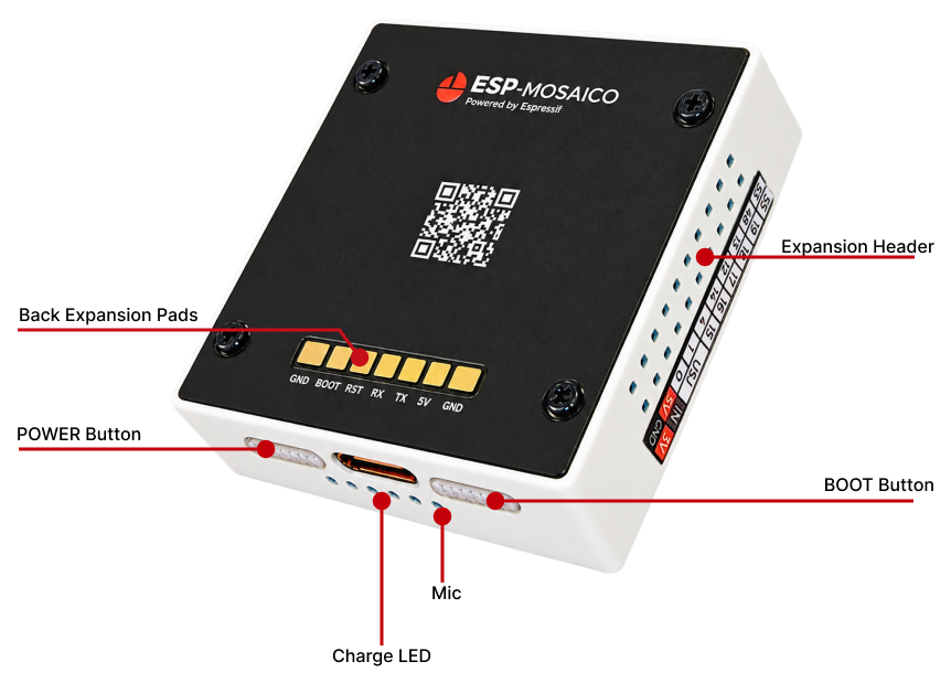
ESP-Mosaico Back (Click to enlarge)
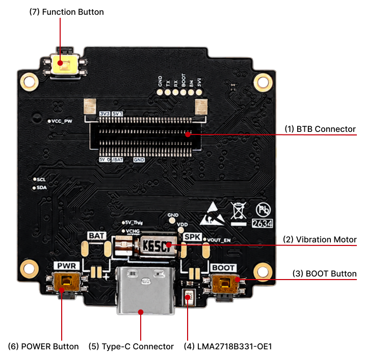
ESP-Mosaico CoreBoard Back (Click to enlarge)
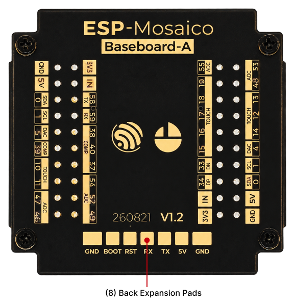
ESP-Mosaico BaseBoard Back (Click to enlarge)
The following describes the main components on the back PCB in clockwise order.
No. |
Key Component |
Description |
|---|---|---|
CoreBoard |
Core board back side, exposing the buttons, Type-C connector, microphone, and vibration motor. |
|
1 |
BTB Connector |
Board-to-board connector mating with the BaseBoard (back side). |
2 |
Vibration Motor |
Vibration motor controlled by GPIO8 (active-high) for haptic feedback. |
3 |
BOOT Button |
Hold during power-up to enter firmware download mode. |
4 |
LMA2718B331-OE1 |
Onboard microphone connected to the ES8311 for voice capture. |
5 |
Type-C Connector |
USB 2.0 High-Speed interface for power, debug/download, and USB communication, with Li-ion charging support. |
6 |
POWER Button |
Single press toggles the device power on/off. |
7 |
Function Button |
Application button (AI button) on GPIO7, active-low. |
BaseBoard |
Base board back side, providing the back expansion pads. |
|
8 |
Back Expansion Pads |
One row of pads silkscreened GND, BOOT, RST, RX, TX, 5V, and GND. They can be used for debug, and the 5V pad can also supply the device. |
Start Application Development
Before powering up, make sure ESP-Mosaico is in good condition.
Required Hardware
ESP-Mosaico
USB cable (data-capable)
Computer (Windows, Linux, or macOS)
Note
Be sure to use a proper USB data cable. Some cables are charge-only and cannot be used for data transfer or programming.
Hardware Notes
Flashing
Connect ESP-Mosaico to the computer with a USB cable through the onboard Type-C port. This port is USB 2.0 High-Speed and supports both power delivery and USB data communication. The native ESP32-S31 chip only supports firmware download through this port in download mode, and does not provide auto-download or log output by itself. The factory firmware integrates a CDC virtual serial port and supports auto-download and serial log output. If flashing fails, try holding the BOOT button while the device is powered off, then power it on to enter download mode. In addition, the left and right module interfaces provide USB Serial/JTAG (left) and a TX/RX UART (right), both of which can be used for debugging and firmware download.
Power
The Type-C port can power the device. The onboard battery is charged at a rated current of 65 mA. When a USB sink device is attached, the Type-C port automatically switches to source mode, with a maximum output of 5 V / 500 mA. If the load exceeds 1 A, the port shuts off automatically and recovers after a period of time. The left and right module interfaces also provide outward 3.3 V and 5 V rails (
3V/5V). These rails are output only when GPIO60 is driven low.VINis an input supply pin that can also charge the onboard battery.
Software Setup
Follow the ESP-IDF Get Started guide to set up the development environment. The target chip for this board is esp32s31.
Note
The board communicates with the PC over USB. Most operating systems (Windows, Linux, macOS) already include the required drivers. If the device is not recognized or the serial connection fails, see Establish Serial Connection with ESP32-S31 for driver installation details.
BSP and Examples
Espressif provides a board support package (BSP) for ESP-Mosaico to simplify initialization of the LCD, touch, audio, sensors, battery, NAND flash, module resources, and USB console.
For the shipped application, buttons, expansion I/O, and getting started, see the ESP-Mosaico User Guide.
Flash the latest firmware in the browser at Firmware Update.
Recommended application framework: ESP-Claw.
After the first successful flash, use the BSP USB CDC console and auto-download support. Typical commands:
idf.py set-target esp32s31
idf.py -p /dev/ttyACM0 flash monitor
Note
The first flash may require manually entering ROM download mode.
The USB device briefly disconnects while the chip resets; IDF Monitor usually reconnects automatically.
Use
monitor --no-resetwhen attaching without restarting the application.Related options:
CONFIG_BSP_USB_CONSOLE,CONFIG_BSP_USB_CONSOLE_AUTO_INIT,CONFIG_BSP_USB_AUTO_DOWNLOAD.
Contents and Packaging
Ordering Information
The development board is available in the variant listed in the table below.
Part Number |
On-board Module |
Flash |
PSRAM |
Antenna |
|---|---|---|---|---|
ESP-Mosaico |
— |
16 MB |
16 MB |
PCB on-board antenna |
For more information about available variants, visit the ESP Product Selector and select the Development Board tab. If you cannot find the variant you need in the table or Product Selector, or if you have special customization requirements, contact Espressif Sales.
Retail Orders
If you order a few samples, each board comes in an individual package in either antistatic bag or any packaging depending on your retailer.
For retail orders, please go to https://www.espressif.com/en/company/contact/buy-a-sample.
Wholesale Orders
If you order in bulk, the boards come in large cardboard boxes.
For wholesale orders, please go to https://www.espressif.com/en/contact-us/sales-questions.
Hardware Reference
Block Diagram
The main components and connections of ESP-Mosaico are shown below.
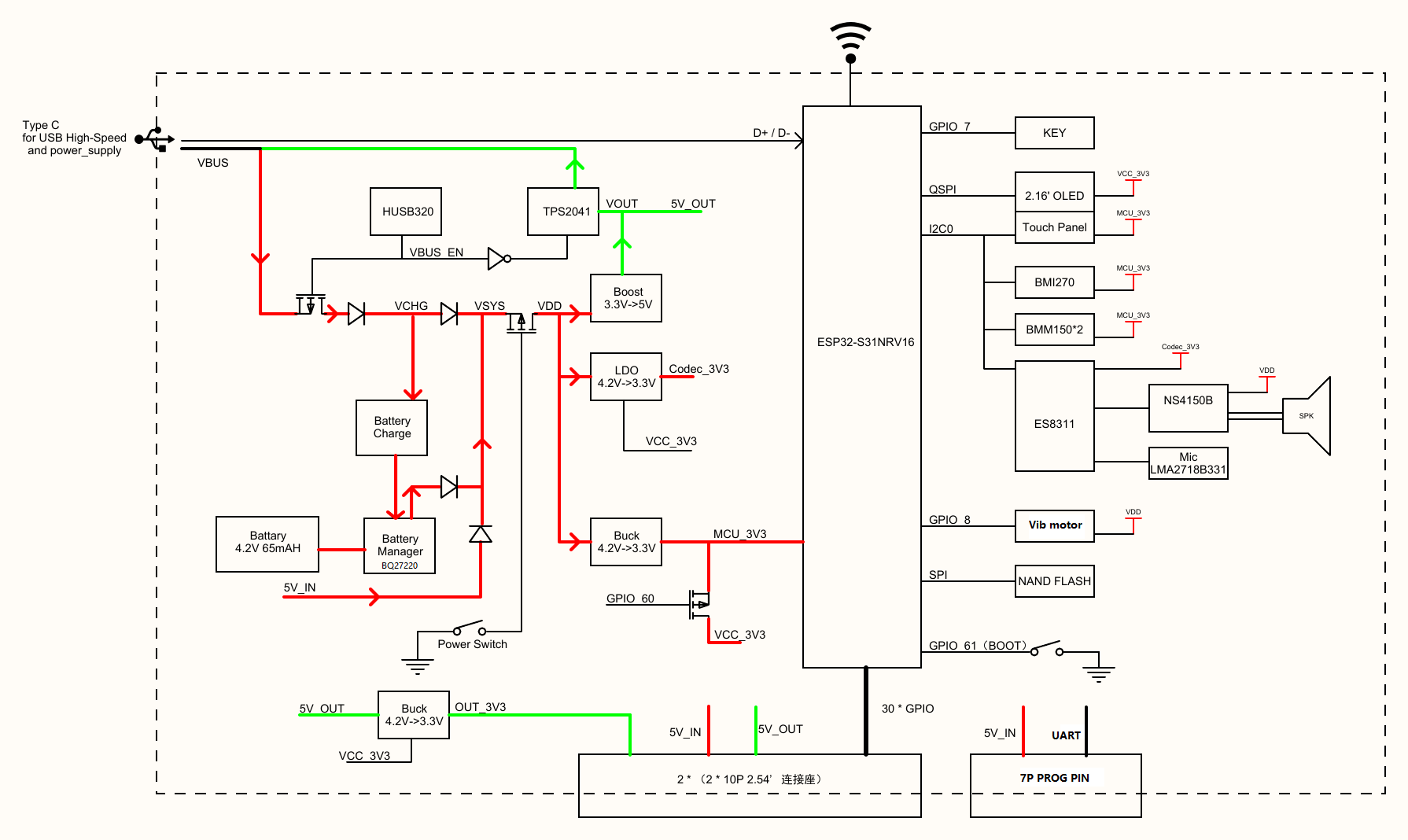
ESP-Mosaico Block Diagram (Click to enlarge)
Power Supply Options
You can power the board in the following ways:
Through the
Type-C (USB-C)portConnect a USB Type-C cable to the Type-C port.
Through the
back expansion padsSupply external power through the back expansion pads on the BaseBoard.
Through the
batteryThe board supports a 3.7 V / 65 mAh Li-ion battery.
Regardless of the power source, use the POWER button to turn the device on or off. External power sources above can also charge the onboard battery.
Type-C Interface
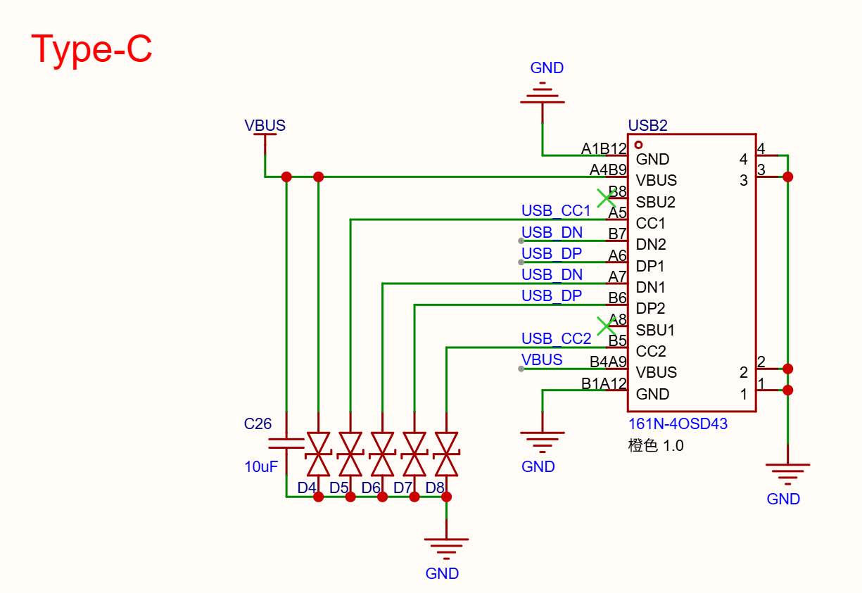
Type-C Interface Schematic (Click to enlarge)
The Type-C port connects to ESP32-S31 USB 2.0 High-Speed OTG for power, debug, and application communication. Onboard USB Serial/JTAG signals are used for download and debugging. The BSP USB CDC console and auto-download feature are the recommended download and log path.
DCDC 3.3 V Circuit
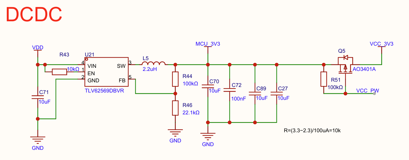
DCDC 3.3 V Schematic (Click to enlarge)
TLV62569 steps VDD down to MCU_3V3, which is then switched to VCC_3V3 by the VCC_PW load switch.
Power-control GPIOs defined by the BSP:
Signal |
GPIO |
Description |
|---|---|---|
VCC_3V3 / VCC_PW |
GPIO60 |
Display supply and 3.3 V / 5 V output control, active-low. |
POWER_SWITCH |
GPIO57 |
Whole-device power-off request; kept high-Z during normal BSP operation, driven open-drain low to request shutdown. |
BOOST Circuit
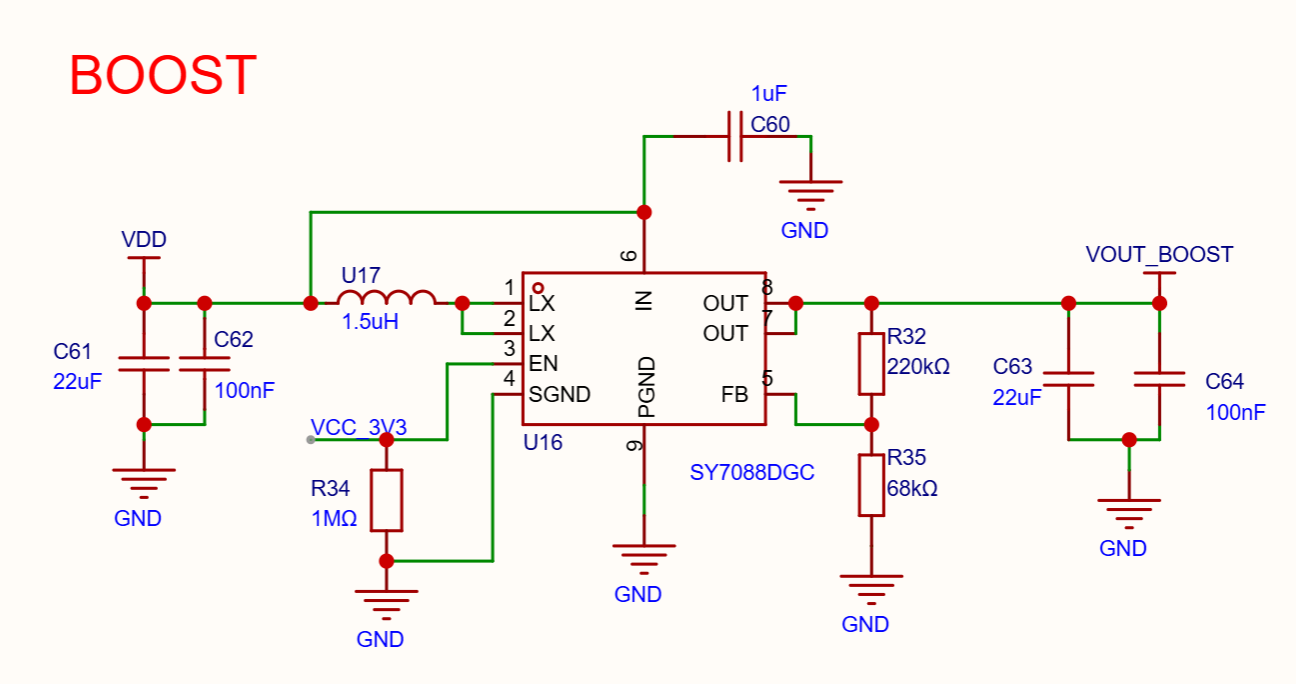
BOOST Schematic (Click to enlarge)
The onboard SY7088 boost converter is enabled by VCC_3V3 and outputs VOUT_BOOST for rails higher than the battery voltage.
Power On/Off Circuit
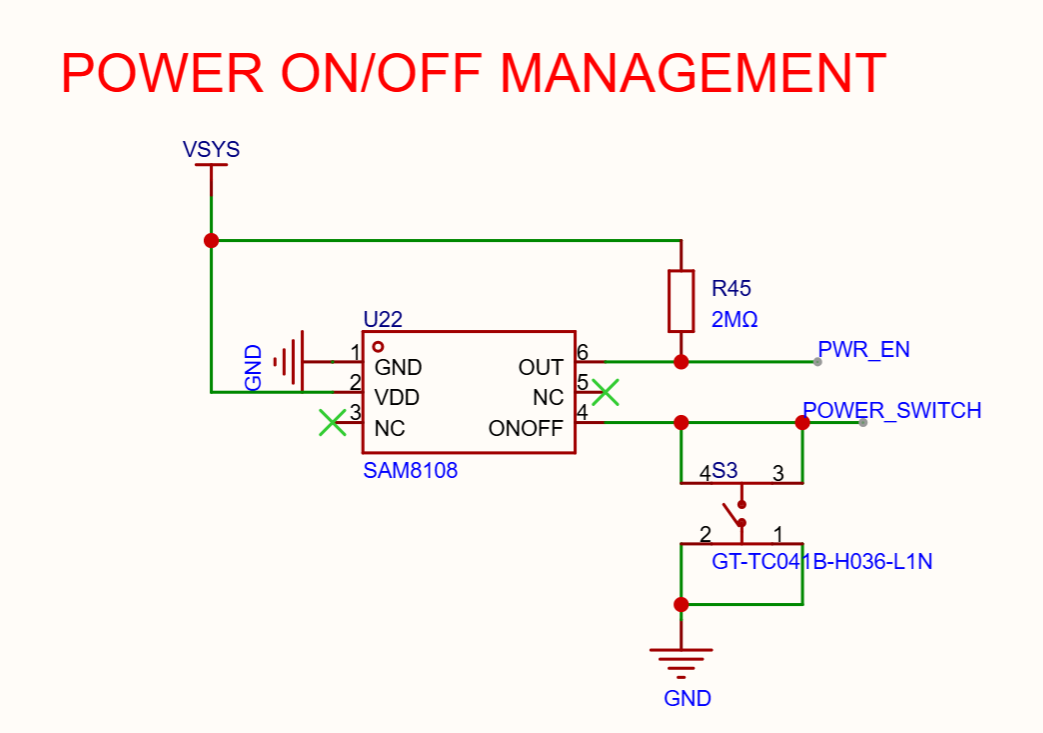
Power On/Off Schematic (Click to enlarge)
SAM8108 works with the POWER button for whole-device power control. The POWER_SWITCH signal can also be monitored or driven by software to request shutdown.
MCU and Pin Assignment
The following table lists the main pin assignments used by the ESP-Mosaico BSP, grouped by function.
Category |
Signal |
GPIO |
Description |
|---|---|---|---|
I2C / Sensors |
I2C0_SDA |
GPIO56 |
Internal I2C0: touch, ES8311, BMI270, BMM150, BQ27220 |
I2C0_SCL |
GPIO3 |
Internal I2C0 clock |
|
I2C1_SDA |
GPIO0 |
External I2C1: module EEPROM and expansion devices |
|
I2C1_SCL |
GPIO1 |
External I2C1 clock |
|
SENSOR_INT |
GPIO2 |
IMU / magnetometer interrupt or signal |
|
TOUCH_INT |
GPIO6 |
Touch interrupt |
|
HMI |
AI_BUTTON |
GPIO7 |
Application button, active-low |
MOTOR |
GPIO8 |
Vibration motor, active-high |
|
LCD |
LCD_DATA3 |
GPIO9 |
CO5300 QSPI DATA3 |
LCD_DATA2 |
GPIO35 |
CO5300 QSPI DATA2 |
|
LCD_DATA0 |
GPIO36 |
CO5300 QSPI DATA0 |
|
LCD_RST |
GPIO44 |
LCD reset |
|
LCD_TE |
GPIO43 |
LCD_TE anti-tearing sync |
|
LCD_SCL |
GPIO42 |
QSPI clock |
|
LCD_CS |
GPIO50 |
LCD chip select |
|
LCD_DATA1 |
GPIO51 |
CO5300 QSPI DATA1 |
|
Audio |
I2S_BCK |
GPIO37 |
Audio bit clock |
I2S_DOUT |
GPIO40 |
Audio data out (DAC) |
|
PA_CTRL |
GPIO45 |
Amplifier enable |
|
I2S_WS |
GPIO49 |
Audio word select |
|
I2S_DIN |
GPIO52 |
Audio data in (ADC) |
|
I2S_MCLK |
GPIO54 |
Audio master clock |
|
Power |
POWER_SWITCH |
GPIO57 |
Power on/off request |
VCC_3V3_CTRL |
GPIO60 |
Display supply and 3.3 V / 5 V output control, active-low |
|
NAND Flash |
NAND_CLK |
GPIO20 |
SPI NAND (SD_D0) |
NAND_D |
GPIO21 |
SPI NAND (SD_D1 / SIO0) |
|
NAND_Q |
GPIO22 |
SPI NAND (SD_D2 / SIO1) |
|
NAND_CS |
GPIO23 |
SPI NAND (SD_D3) |
|
NAND_HOLD |
GPIO24 |
SPI NAND (SD_CLK / SIO3) |
|
NAND_WP |
GPIO25 |
SPI NAND (SD_CMD / SIO2) |
I2C Device Addresses
V1.2 splits onboard devices and expansion modules onto two I2C buses:
I2C0 (internal):
I2C0_SDA= GPIO56,I2C0_SCL= GPIO3, connecting touch, audio codec, IMU, magnetometers, and the fuel gauge.I2C1 (external):
I2C1_SDA= GPIO0,I2C1_SCL= GPIO1, connecting module EEPROM and other external devices.
Internal I2C0 (7-bit addresses)
I2C Address |
Device |
Description |
|---|---|---|
0x11 |
BMM150 #2 |
Onboard 3-axis magnetometer |
0x12 |
BMM150 #3 |
Onboard 3-axis magnetometer |
0x19 |
ES8311 |
Onboard audio codec |
0x55 |
BQ27220 |
Onboard fuel gauge |
0x5A |
CST9220 |
Onboard touch controller |
0x69 |
BMI270 |
Onboard 6-axis IMU |
External I2C1 (7-bit addresses)
Module EEPROMs are on the attached modules, not on the mainboard, and appear only when a module with EEPROM is plugged into the corresponding slot.
I2C Address |
Device |
Description |
|---|---|---|
0x50 |
Module EEPROM (Left) |
On the left module, not the mainboard; selected when GPIO14 is driven low |
0x51 |
Module EEPROM (Right) |
On the right module, not the mainboard; selected when GPIO39 is driven high |
LCD Interface
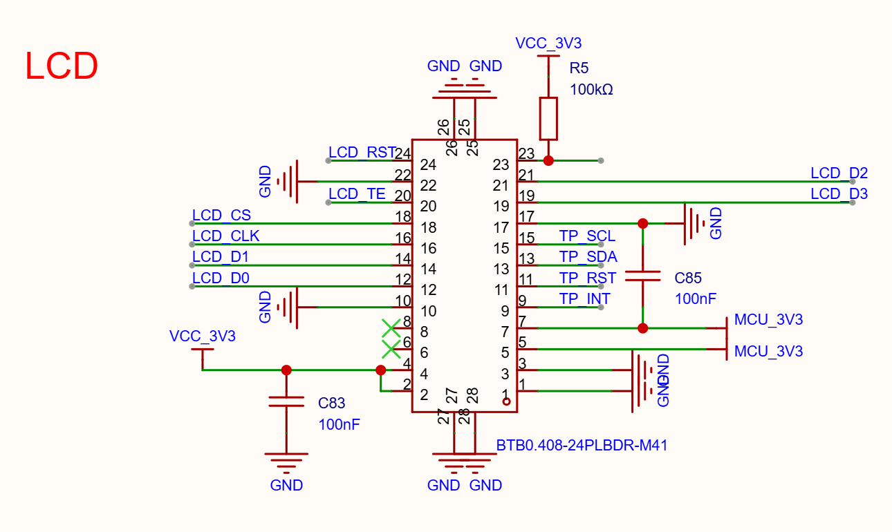
LCD Interface Schematic (Click to enlarge)
LCD driver: CO5300, QSPI interface, 480 × 480 resolution.
Touch controller: CST9220 series, I2C interface (
TP_SCL/TP_SDA/TP_RST/TP_INT).
Vibration Motor Interface
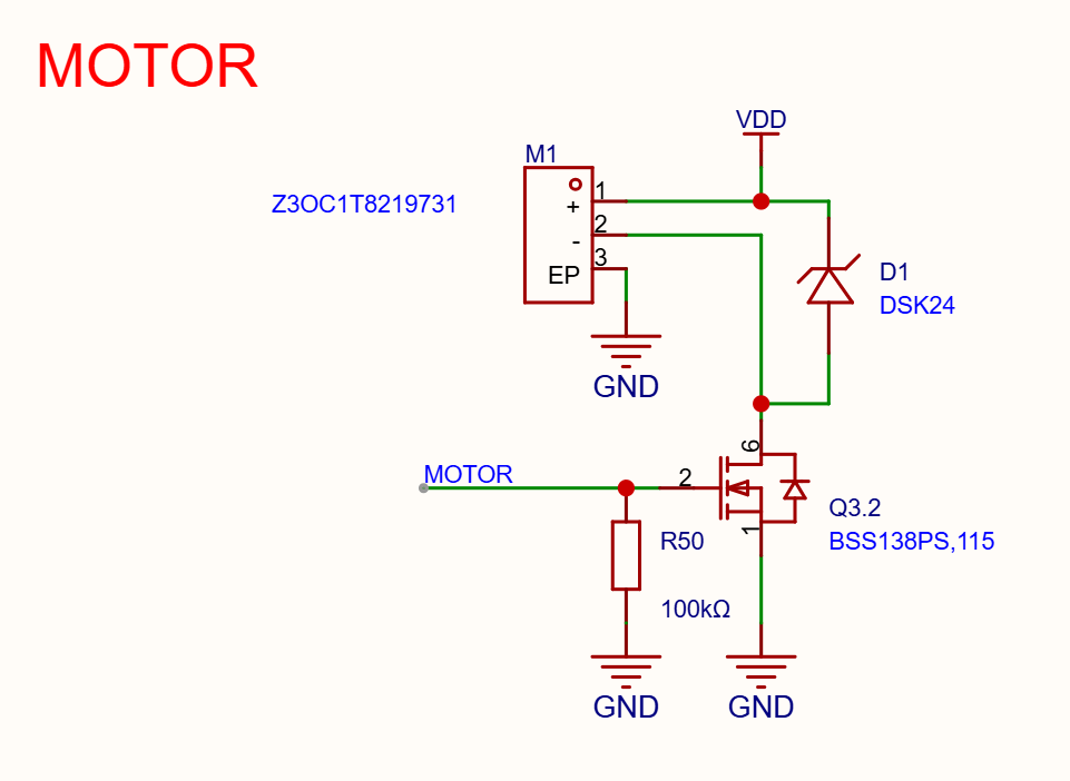
Vibration Motor Schematic (Click to enlarge)
The vibration motor is driven by MOTOR (GPIO8) through a low-side MOSFET, active-high.
Module Interface
The BaseBoard provides two 2 × 10P, 2.54 mm pitch expansion headers (H2 left and H1 right) that expose GPIOs, UART, USB Serial/JTAG, power, and ground for secondary development. Except for power and ground, all expansion signal pins support GPIO and can be flexibly remapped through the GPIO matrix. Labels such as ADC / TOUCH / COMP / DAC in the tables below mark the pin’s analog capabilities and do not prevent using it as a general-purpose GPIO.
ESP-Mosaico provides left and right module slots. The BSP discovers them through EEPROM address selection:
Slot |
EEPROM Address |
Description |
|---|---|---|
Left ( |
0x50 |
Address-select GPIO14, driven low |
Right ( |
0x51 |
Address-select GPIO39, driven high; mounted 180° relative to the left slot |
Left Module Slot (H2) Pins
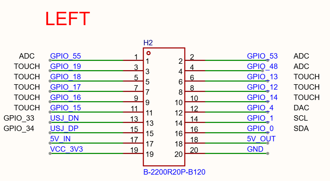
Left Module Interface Schematic (Click to enlarge)
Pins are listed clockwise around the connector, starting from Pin1 (odd-numbered row first, then even-numbered row back).
Pin |
Signal |
Description |
|---|---|---|
1 |
GPIO55 |
ADC |
3 |
GPIO19 |
ADC |
5 |
GPIO18 |
TOUCH |
7 |
GPIO17 |
TOUCH |
9 |
GPIO16 |
TOUCH |
11 |
GPIO15 |
TOUCH |
13 |
USJ_DN (GPIO33) |
USB Serial/JTAG D- |
15 |
USJ_DP (GPIO34) |
USB Serial/JTAG D+ |
17 |
5V_IN |
External 5 V input (can power and charge the device) |
19 |
VCC_3V3 |
3.3 V output (controlled by GPIO60) |
20 |
GND |
Ground |
18 |
5V_OUT |
5 V output (controlled by GPIO60) |
16 |
GPIO0 |
SDA (external I2C1) |
14 |
GPIO1 |
SCL (external I2C1) |
12 |
GPIO4 |
DAC |
10 |
GPIO14 |
TOUCH; EEPROM address select |
8 |
GPIO12 |
TOUCH |
6 |
GPIO13 |
TOUCH |
4 |
GPIO48 |
ADC |
2 |
GPIO53 |
ADC |
Right Module Slot (H1) Pins
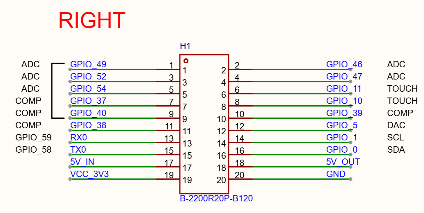
Right Module Interface Schematic (Click to enlarge)
Pins are listed clockwise around the connector, starting from Pin1 (odd-numbered row first, then even-numbered row back).
Pin |
Signal |
Description |
|---|---|---|
1 |
GPIO49 * |
ADC; multiplexed with codec |
3 |
GPIO52 * |
ADC; multiplexed with codec |
5 |
GPIO54 * |
ADC; multiplexed with codec |
7 |
GPIO37 * |
COMP; multiplexed with codec |
9 |
GPIO40 * |
COMP; multiplexed with codec |
11 |
GPIO38 |
COMP |
13 |
RX0 (GPIO59) |
UART RX |
15 |
TX0 (GPIO58) |
UART TX |
17 |
5V_IN |
External 5 V input (can power and charge the device) |
19 |
VCC_3V3 |
3.3 V output (controlled by GPIO60) |
20 |
GND |
Ground |
18 |
5V_OUT |
5 V output (controlled by GPIO60) |
16 |
GPIO0 |
SDA (external I2C1) |
14 |
GPIO1 |
SCL (external I2C1) |
12 |
GPIO5 |
DAC |
10 |
GPIO39 |
TOUCH; EEPROM address select |
8 |
GPIO10 |
TOUCH |
6 |
GPIO11 |
TOUCH |
4 |
GPIO47 |
ADC |
2 |
GPIO46 |
ADC |
Important
Pins marked with * (5 in total) are multiplexed with the onboard audio codec I2S bus: GPIO49 (I2S_WS), GPIO52 (I2S_DIN), GPIO54 (I2S_MCLK), GPIO37 (I2S_BCK), and GPIO40 (I2S_DOUT). These pins can be used for module expansion only when codec audio is not required. Do not use them for expansion if the application still needs the onboard ES8311 / speaker / microphone path.
Note
When the left camera module claims DVP pins, GPIO14 (EEPROM address-select) is reused as DVP D4 and EEPROM access to that slot is suspended until the camera resource is released. See ESP-Mosaico Camera Module and ESP-Mosaico Multi-function Interaction Module for the camera module and multi-function interaction module.
Hardware Revision Details
V1.2 (this document): Major changes compared with V1.0 are as follows.
Display interface:
LCD_RSTandLCD_SCLare swapped (V1.2:LCD_RST= GPIO44,LCD_SCL= GPIO42).The charge LED colors are changed: V1.0 uses red while charging and green when fully charged; V1.2 uses orange while charging and white when fully charged.
The programmable orange LED (formerly GPIO3) is removed.
The 3.3 V power LED is removed.
Independent codec power-domain control (formerly GPIO56) is removed.
Onboard devices and expansion modules use two I2C buses: internal I2C0 (SDA = GPIO56, SCL = GPIO3); external I2C1 remains SDA = GPIO0, SCL = GPIO1.
The external 3.3 V rail is generated by a dedicated DCDC, so expansion modules do not affect the internal MCU supply.
V1.0: See ESP-Mosaico V1.0.
Disclaimer and Copyright Notice
Please refer to the Disclaimer and Copyright Notice.