Schematic Checklist
Overview
The integrated circuitry of ESP32-C6 requires only 20 electrical components (resistors, capacitors, and inductors) and a crystal, as well as an SPI flash (not needed for QFN32 package). The high integration of ESP32-C6 allows for simple peripheral circuit design. This chapter details the schematic design of ESP32-C6.
The following figure shows a reference schematic design of ESP32-C6. It can be used as the basis of your schematic design.
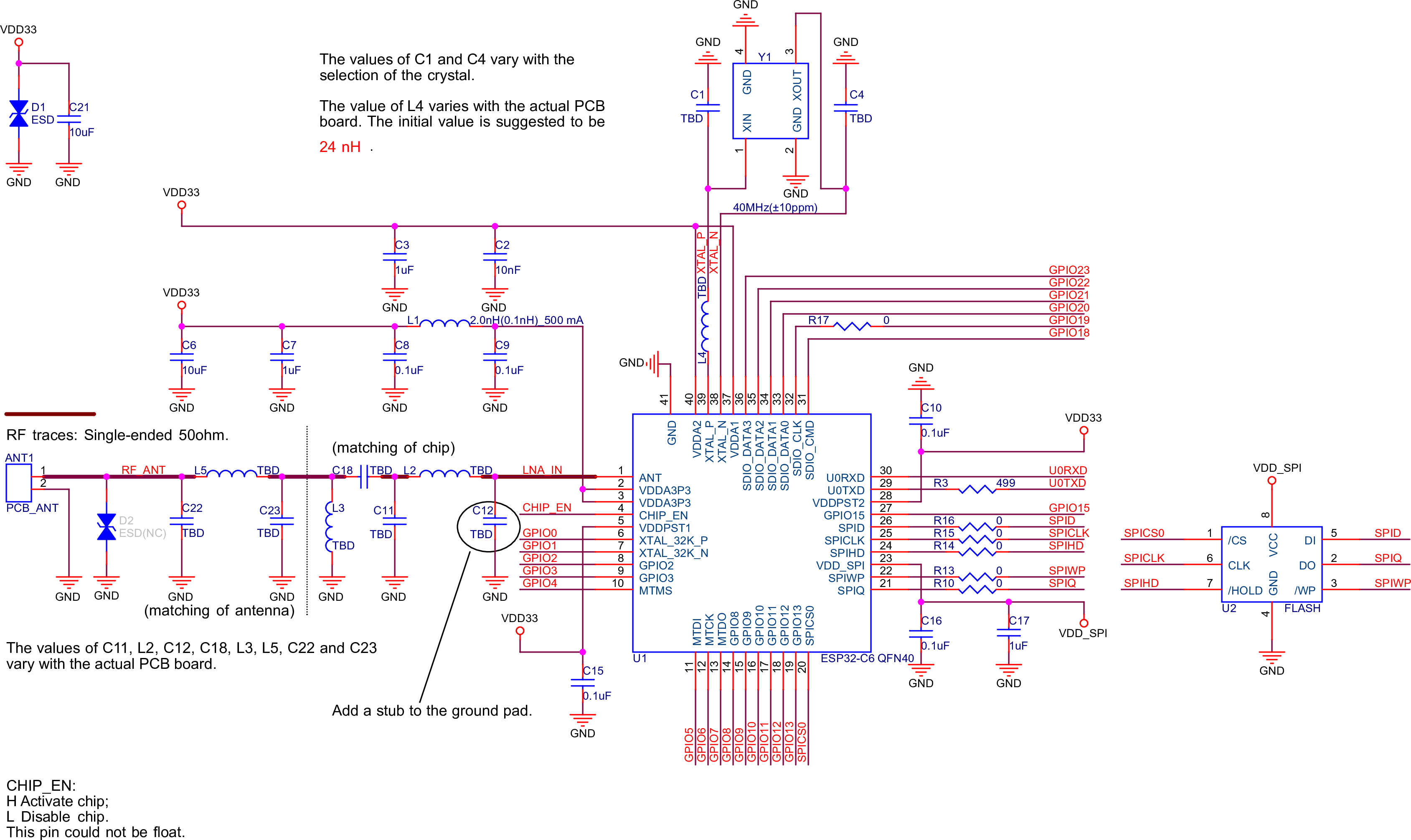
ESP32-C6 Reference Schematic for QFN40 Package
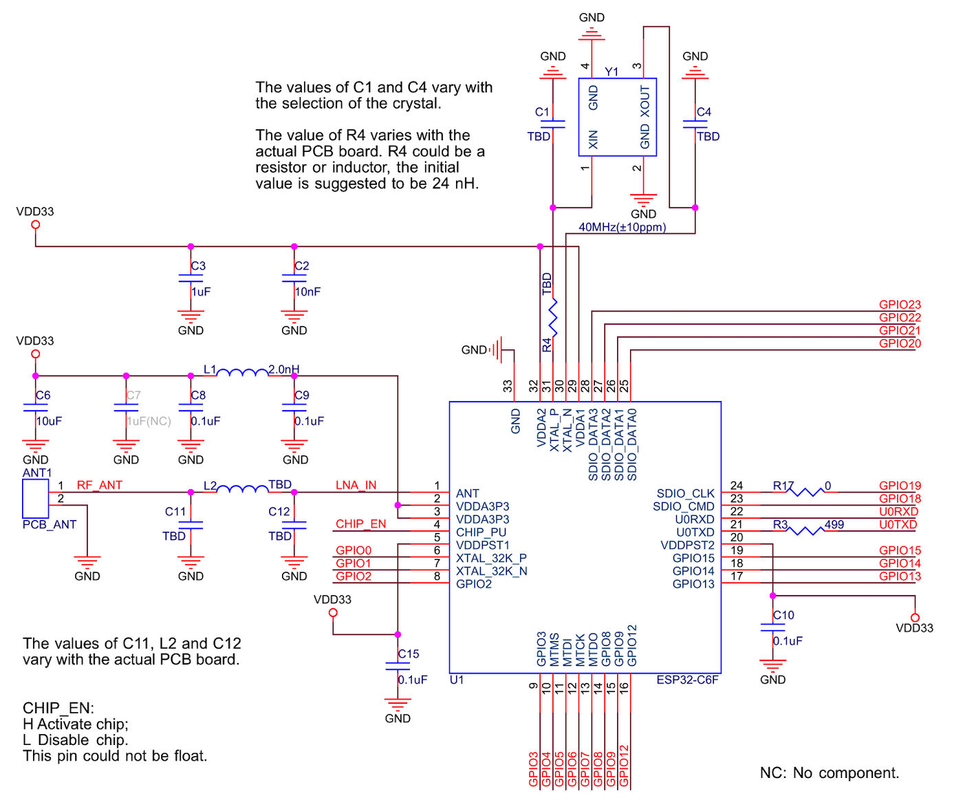
ESP32-C6 Reference Schematic for QFN32 Package
Note
ESP32-C6 consists of variants in two packages, namely the QFN40 package and the QFN32 package. The main difference between these two packages is whether the flash is integrated into the chip’s package.
Unless otherwise specified, “ESP32-C6” used in this document refers to the QFN40 variant.
Any basic ESP32-C6 circuit design may be broken down into the following major building blocks:
The rest of this chapter details the specifics of circuit design for each of these sections.
Power Supply
The general recommendations for power supply design are:
When using a single power supply, the recommended power supply voltage is 3.3 V and the output current is no less than 500 mA.
It is suggested to add an ESD protection diode and at least 10 μF capacitor at the main power entrance (where the external power supply enters the PCB).
The power scheme is shown in Figure ESP32-C6 Power Scheme.
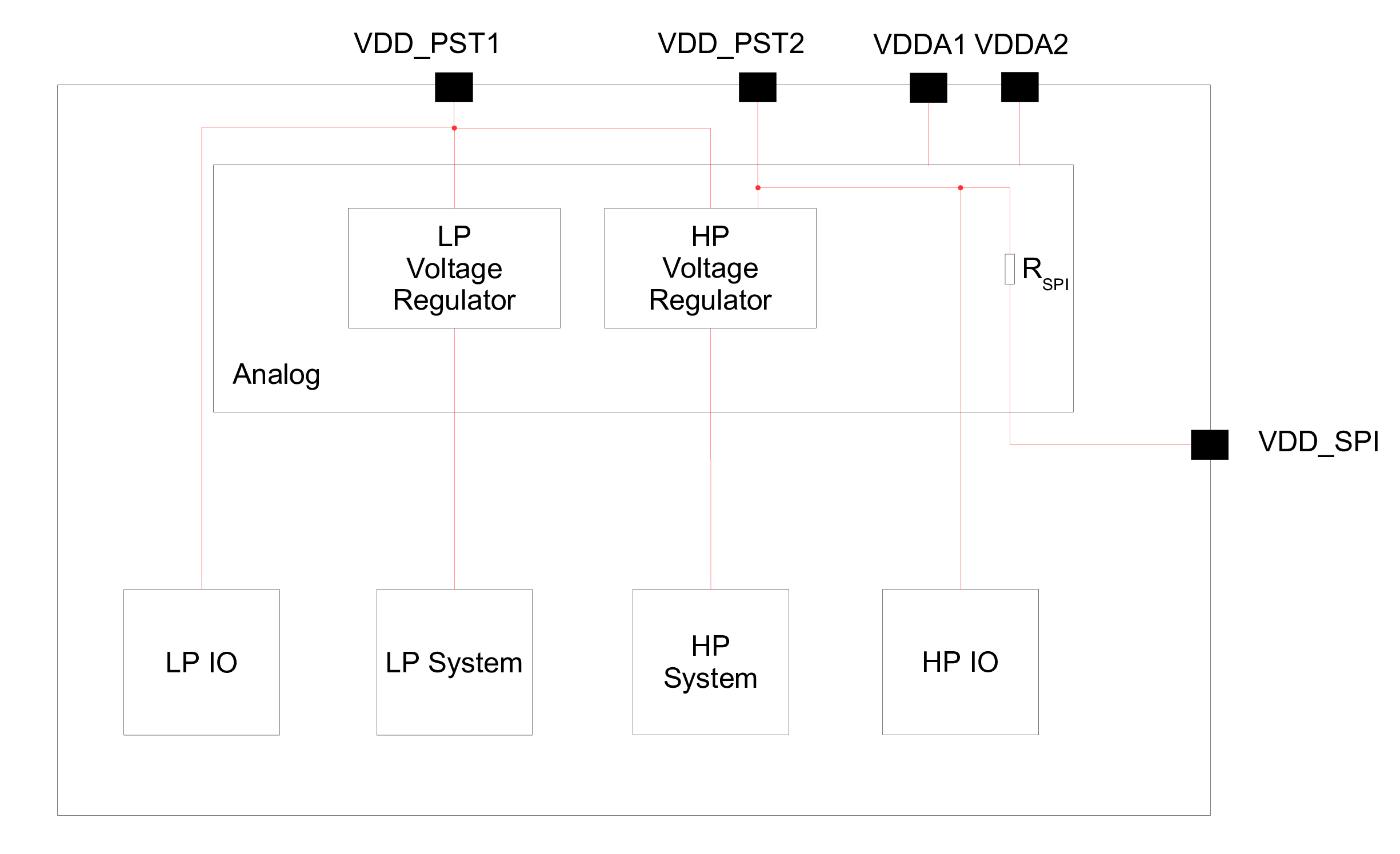
ESP32-C6 Power Scheme
More information about power supply pins can be found in ESP32-C6 Series Datasheet > Section Power Supply.
Digital Power Supply
ESP32-C6 has pin5 VDDPST1 and pin28 VDDPST2 as the digital power supply pin(s) working in a voltage range of 3.0 V ~ 3.6 V. It is recommended to add an extra 0.1 μF decoupling capacitor close to the pin(s).
Pin VDD_SPI (pin23) can serve as the power supply for the external device at 3.3 V (typical value), provided by VDDPST2 via RSPI. Therefore, there will be some voltage drop from VDDPST2. When the VDD_SPI outputs 3.3 V, it is recommended that users add 0.1 μF and 1 μF capacitors close to VDD_SPI.
VDD_SPI can be connected to and powered by an external power supply.
When not serving as a power supply pin, VDD_SPI can be used as a regular GPIO.
It is recommended to use the VDD_SPI to power the in-package or off-package flash.
Attention
When using VDD_SPI as the power supply pin for the in-package flash/PSRAM or external 3.3 V flash, considering the voltage drop mentioned above, VDDPST2 should be 3.0 V or above, so as to meet the requirements of flash’s working voltage.
Analog Power Supply
ESP32-C6’s VDDA and VDDA3P3 pins are the analog power supply pins, working at 3.0 V ~ 3.6 V.
For VDDA3P3, when ESP32-C6 is transmitting signals, there may be a sudden increase in the current draw, causing power rail collapse. Therefore, it is highly recommended to add a 10 μF capacitor to the power rail, which can work in conjunction with the 1 μF capacitor(s) or other capacitors.
It is suggested to add an extra 10 μF capacitor at the main power entrance. If the main power entrance is close to VDDA3P3, then the two 10 μF capacitors can be merged into one.
Add an LC circuit to the VDDA3P3 power rail to suppress high-frequency harmonics. The inductor’s rated current is preferably 500 mA and above.
For the remaining capacitor circuits, please refer to ESP32-C6 Reference Schematic for QFN40 Package.
Chip Power-up and Reset Timing
ESP32-C6’s CHIP_PU pin can enable the chip when it is high and reset the chip when it is low.
When ESP32-C6 uses a 3.3 V system power supply, the power rails need some time to stabilize before CHIP_PU is pulled up and the chip is enabled. Therefore, CHIP_PU needs to be asserted high after the 3.3 V rails have been brought up.
To reset the chip, keep the reset voltage VIL_nRST in the range of (–0.3 ~ 0.25 × VDDPST1) V. To avoid reboots caused by external interferences, make the CHIP_PU trace as short as possible.
Figure ESP32-C6 Power-up and Reset Timing shows the power-up and reset timing of ESP32-C6.
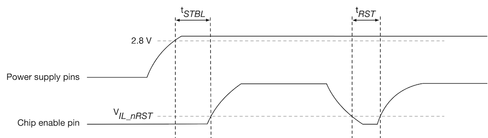
ESP32-C6 Power-up and Reset Timing
Table Description of Timing Parameters for Power-up and Reset provides the specific timing requirements.
Parameter |
Description |
Minimum (µs) |
|---|---|---|
tSTBL |
Time reserved for the power rails to stabilize before the CHIP_PU pin is pulled high to activate the chip |
50 |
tRST |
Time reserved for CHIP_PU to stay below VIL_nRST to reset the chip |
50 |
Attention
CHIP_PU must not be left floating.
To ensure the correct power-up and reset timing, it is advised to add an RC delay circuit at the CHIP_PU pin. The recommended setting for the RC delay circuit is usually R = 10 kΩ and C = 1 μF. However, specific parameters should be adjusted based on the characteristics of the actual power supply and the power-up and reset timing of the chip.
If the user application has one of the following scenarios:
Slow power rise or fall, such as during battery charging.
Frequent power on/off operations.
Unstable power supply, such as in photovoltaic power generation.
Then, the RC circuit alone may not meet the timing requirements, which may prevent the chip from entering normal operating mode or cause flash erase operations to occasionally fail to complete. In this case, please reserve a power monitor chip to reset the chip when the power supply is abnormal, and the threshold of the power monitor chip is recommended to be around 3.0 V.
Flash
ESP32-C6 requires in-package or off-package flash to store application firmware and data.
In-Package Flash
ESP32-C6 series of chips have in-package 4 MB or 8 MB flash. The pins for flash are not bonded out.
Off-Package Flash
To reduce the risk of software compatibility issues, it is recommended to use flash models officially validated by Espressif. For detailed model selection, consult the sales or technical support team. It is recommended to add zero-ohm resistor footprints in series on the SPI communication lines as shown in Figure ESP32-C6 Schematic for External Flash. These footprints provide flexibility for future adjustments, such as tuning drive strength, mitigating RF interference, correcting signal timing, and reducing noise, if needed.
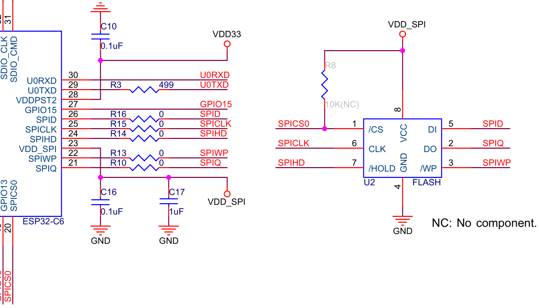
ESP32-C6 Schematic for External Flash
Clock Source
ESP32-C6 supports two external clock sources:
External Crystal Clock Source (Compulsory)
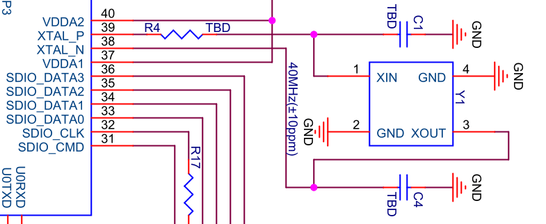
The ESP32-C6 firmware only supports 40 MHz crystal.
The circuit for the crystal is shown in Figure ESP32-C6 Schematic for External Crystal. Note that the accuracy of the selected crystal should be within ±10 ppm.
ESP32-C6 Schematic for External Crystal
Please add a series component on the XTAL_P clock trace. Initially, it is suggested to use an inductor of 24 nH to reduce the impact of high-frequency crystal harmonics on RF performance, and the value should be adjusted after an overall test.
The initial values of external capacitors C1 and C4 can be determined according to the formula:
where the value of CL (load capacitance) can be found in the crystal’s datasheet, and the value of Cstray refers to the PCB’s stray capacitance. The values of C1 and C4 need to be further adjusted after an overall test as below:
Select TX tone mode using the Certification and Test Tool.
Observe the 2.4 GHz signal with a radio communication analyzer or a spectrum analyzer and demodulate it to obtain the actual frequency offset.
Adjust the frequency offset to be within ±10 ppm (recommended) by adjusting the external load capacitance.
When the center frequency offset is positive, it means that the equivalent load capacitance is small, and the external load capacitance needs to be increased.
When the center frequency offset is negative, it means the equivalent load capacitance is large, and the external load capacitance needs to be reduced.
External load capacitance at the two sides are usually equal, but in special cases, they may have slightly different values.
Note
Defects in the manufacturing of crystal (for example, large frequency deviation of more than ±10 ppm, unstable performance within the operating temperature range, etc) may lead to the malfunction of ESP32-C6, resulting in a decrease of the RF performance.
It is recommended that the amplitude of the crystal is greater than 500 mV.
When Wi-Fi or Bluetooth connection fails, after ruling out software problems, you may follow the steps mentioned above to ensure that the frequency offset meets the requirements by adjusting capacitors at the two sides of the crystal.
RTC Clock Source (Optional)
ESP32-C6 supports an external 32.768 kHz crystal to act as the RTC clock. The external RTC clock source enhances timing accuracy and consequently decreases average power consumption, without impacting functionality.
Figure ESP32-C6 Schematic for 32.768 kHz Crystal shows the schematic for the external 32.768 kHz crystal.
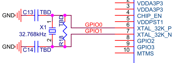
ESP32-C6 Schematic for 32.768 kHz Crystal
Please note the requirements for the 32.768 kHz crystal:
Equivalent series resistance (ESR) ≤ 70 kΩ.
Load capacitance at both ends should be configured according to the crystal’s specification.
The parallel resistor R is used for biasing the crystal circuit (5 MΩ < R ≤ 10 MΩ).
In general, you do not need to populate the resistor.
If the RTC clock source is not required, then the pins for the 32.768 kHz crystal can be used as GPIOs.
RF
RF Circuit
ESP32-C6’s RF circuit is mainly composed of three parts, the RF traces on the PCB board, the chip matching circuit, the antenna and the antenna matching circuit. Each part should meet the following requirements:
For the RF traces on the PCB board, 50 Ω impedance control is required.
For the chip matching circuit, it must be placed close to the chip. A CLCCL structure is preferred.
The CLCCL structure forms a bandpass filter, which is mainly used to adjust impedance points, suppress high-frequency harmonics, and suppress low-frequency noise.
The RF matching circuit is shown in Figure ESP32-C6 Schematic for RF Matching.
For the antenna and the antenna matching circuit, to ensure radiation performance, the antenna’s characteristic impedance must be around 50 Ω. Adding a CLC matching circuit near the antenna is recommended to adjust the antenna. However, if the available space is limited and the antenna impedance point can be guaranteed to be 50 Ω by simulation, then there is no need to add a matching circuit near the antenna.
It is recommended to include ESD protection devices for the antenna to mitigate electrostatic interference.
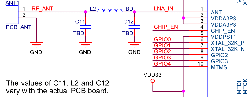
ESP32-C6 Schematic for RF Matching
RF Tuning
The RF matching parameters vary with the board, so the ones used in Espressif modules could not be applied directly. Follow the instructions below to do RF tuning.
Figure ESP32-C6 RF Tuning Diagram shows the general process of RF tuning.
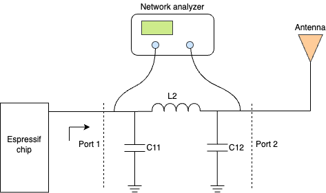
ESP32-C6 RF Tuning Diagram
In the matching circuit, define the port near the chip as Port 1 and the port near the antenna as Port 2. S11 describes the ratio of the signal power reflected back from Port 1 to the input signal power, the transmission performance is best if the matching impedance is conjugate to the chip impedance. S21 is used to describe the transmission loss of signal from Port 1 to Port 2. If S11 is close to the chip conjugate point 35+j0 and S21 is less than -35 dB at 4.8 GHz and 7.2 GHz, the matching circuit can satisfy transmission requirements.
Connect the two ends of the matching circuit to the network analyzer, and test its signal reflection parameter S11 and transmission parameter S21. Adjust the values of the components in the circuit until S11 and S21 meet the requirements. If your PCB design of the chip strictly follows the PCB design stated in Chapter PCB Layout Design, you can refer to the value ranges in Table Recommended Value Ranges for Components to debug the matching circuit.
Reference Designator |
Recommended Value Range |
Serial No. |
|---|---|---|
C11 |
1.2 ~ 1.8 pF |
GRM0335C1H1RXBA01D |
L2 |
2.0 ~ 3.0 nH |
LQP03TN2NXB02D |
C12 |
1.8 ~ 1.2 pF |
GRM0335C1H1RXBA01D |
Please use 0201 packages for RF matching components and add a stub to the first capacitor in the matching circuit at the chip end.
Note
If RF function is not required, it is recommended not to initialize the RF stack in firmware. In this case, the RF pin can be left floating. However, if RF function is enabled, make sure an antenna is connected. Operation without an antenna may result in unstable behavior or potential damage to the RF circuit.
UART
ESP32-C6 includes 3 UART interfaces, UART0, UART1, and LP UART. U0TXD and U0RXD are GPIO16 and GPIO17 by default. Other UART signals can be mapped to any available GPIOs by software configurations.
LP UART pin configurations are shown in Table LP UART Pin Configurations.
Usually, UART0 is used as the serial port for download and log printing. For instructions on download over UART0, please refer to Section Download Guidelines. It is recommended to connect a 499 Ω series resistor to the U0TXD line to suppress harmonics.
For application communication, use UART interfaces other than UART0 if possible. Add a series resistor on the TX line to suppress harmonics.
When using the AT firmware, please note that the UART GPIO is already configured (refer to Hardware Connection). It is recommended to use the default configuration.
Signal |
Pin |
|---|---|
LP_UART_DTRN |
XTAL_32K_P |
LP_UART_DSRN |
XTAL_32K_N |
LP_UART_RTSN |
GPIO2 |
LP_UART_CTSN |
GPIO3 |
LP_UART_RXD |
MTMS |
LP_UART_TXD |
MTDI |
SPI
When using the SPI function, to improve EMC performance, add a series resistor (or ferrite bead) and a capacitor to ground on the SPI_CLK trace. If space allows, it is recommended to also add a series resistor and capacitor to ground on other SPI traces. Ensure that the RC/LC components are placed close to the pins of the chip or module.
Strapping Pins
At each startup or reset, a chip requires some initial configuration parameters, such as in which boot mode to load the chip, etc. These parameters are passed over via the strapping pins. After reset, the strapping pins work as normal function pins.
GPIO8, GPIO9, GPIO15, MTMS, and MTDI are strapping pins.
All the information about strapping pins is covered in ESP32-C6 Series Datasheet > Chapter Boot Configurations.
In this section, we will mainly cover the strapping pins related to boot mode.
After chip reset is released, the combination of GPIO8 and GPIO9 controls the boot mode. See Table Boot Mode Control.
Boot Mode |
GPIO8 |
GPIO9 |
|---|---|---|
Default Config |
– (Floating) |
1 (Pull-up) |
SPI Boot (default) |
Any value |
1 |
Download Boot |
1 |
0 |
Invalid combination [1] |
0 |
0 |
Signals applied to the strapping pins should have specific setup time and hold time. For more information, see Figure Setup and Hold Times for Strapping Pins and Table Description of Timing Parameters for Strapping Pins.
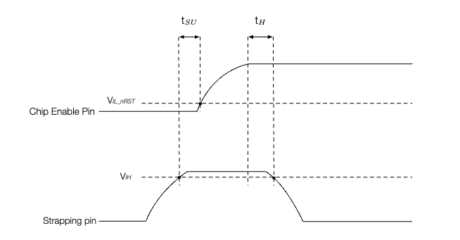
Setup and Hold Times for Strapping Pins
Parameter |
Description |
Minimum (ms) |
|---|---|---|
tSU |
Time reserved for the power rails to stabilize before the chip enable pin (CHIP_PU) is pulled high to activate the chip. |
0 |
tH |
Time reserved for the chip to read the strapping pin values after CHIP_PU is already high and before these pins start operating as regular IO pins. |
3 |
Attention
It is recommended to place a pull-up resistor at the GPIO9 pin.
Do not add high-value capacitors at GPIO9, or the chip may enter download mode.
GPIO
The pins of ESP32-C6 can be configured via IO MUX or GPIO matrix. IO MUX provides the default pin configurations (see ESP32-C6 Series Datasheet > Appendix ESP32-C6 Consolidated Pin Overview), whereas the GPIO matrix is used to route signals from peripherals to GPIO pins. For more information about IO MUX and GPIO matrix, please refer to ESP32-C6 Technical Reference Manual > Chapter IO MUX and GPIO Matrix.
Some peripheral signals have already been routed to certain GPIO pins, while some can be routed to any available GPIO pins. For details, please refer to ESP32-C6 Series Datasheet > Section Peripherals.
When using GPIOs, please:
Pay attention to the states of strapping pins during power-up.
Pay attention to the default GPIO configurations after reset (see the table below). For unused pins in the high-impedance state without an internal pull-up or pull-down, it is recommended to add a pull-up or pull-down resistor or enable the internal pull during software initialization to avoid extra power consumption, selecting the direction as required by the external circuit.
Avoid using the pins already occupied by flash.
Only GPIOs in the VDDPST1 power domain can be controlled in Deep-sleep mode.
Pin No |
Pin Name |
Pin Providing Power |
At Reset |
After Reset |
|---|---|---|---|---|
1 |
ANT |
|||
2 |
VDDA3P3 |
|||
3 |
VDDA3P3 |
|||
4 |
CHIP_PU |
|||
5 |
VDDPST1 |
|||
6 |
XTAL_32K_P |
VDDPST1 |
||
7 |
XTAL_32K_N |
VDDPST1 |
||
8 |
GPIO2 |
VDDPST1 |
IE |
IE |
9 |
GPIO3 |
VDDPST1 |
IE |
IE |
10 |
MTMS |
VDDPST1 |
IE |
IE |
11 |
MTDI |
VDDPST1 |
IE |
IE |
12 |
MTCK |
VDDPST1 |
IE, WPU |
|
13 |
MTDO |
VDDPST1 |
IE |
|
14 |
GPIO8 |
VDDPST2 |
IE |
IE |
15 |
GPIO9 |
VDDPST2 |
IE, WPU |
IE, WPU |
16 |
GPIO10 |
VDDPST2 |
IE |
|
17 |
GPIO11 |
VDDPST2 |
IE |
|
18 |
GPIO12 |
VDDPST2 |
IE |
|
19 |
GPIO13 |
VDDPST2 |
IE, WPU |
|
20 |
SPICS0 |
VDD_SPI |
WPU |
IE, WPU |
21 |
SPIQ |
VDD_SPI |
WPU |
IE, WPU |
22 |
SPIWP |
VDD_SPI |
WPU |
IE, WPU |
23 |
VDD_SPI |
|||
24 |
SPIHD |
VDD_SPI |
WPU |
IE, WPU |
25 |
SPICLK |
VDD_SPI |
WPU |
IE, WPU |
26 |
SPID |
VDD_SPI |
WPU |
IE, WPU |
27 |
GPIO15 |
VDDPST2 |
IE |
IE |
28 |
VDDPST2 |
|||
29 |
U0TXD |
VDDPST2 |
WPU |
|
30 |
U0RXD |
VDDPST2 |
IE, WPU |
|
31 |
SDIO_CMD |
VDDPST2 |
WPU |
IE |
32 |
SDIO_CLK |
VDDPST2 |
WPU |
IE |
33 |
SDIO_DATA0 |
VDDPST2 |
WPU |
IE |
34 |
SDIO_DATA1 |
VDDPST2 |
WPU |
IE |
35 |
SDIO_DATA2 |
VDDPST2 |
WPU |
IE |
36 |
SDIO_DATA3 |
VDDPST2 |
WPU |
IE |
37 |
VDDA1 |
|||
38 |
XTAL_N |
|||
39 |
XTAL_P |
|||
40 |
VDDA2 |
|||
41 |
GND |
IE – input enabled
WPU – internal weak pull-up resistor enabled
WPD – internal weak pull-down resistor enabled
USB_PU – USB pull-up resistor enabled
By default, the USB function is enabled for USB pins (i.e., GPIO12 and GPIO13), and the pin pull-up is decided by the USB pull-up resistor. The USB pull-up resistor is controlled by
USB_SERIAL_JTAG_DP/DM_PULLUPand the pull-up value is controlled byUSB_SERIAL_JTAG_PULLUP_VALUE. For details, see ESP32-C6 Technical Reference Manual > Chapter USB Serial/JTAG Controller.When the USB function is disabled, USB pins are used as regular GPIOs. At reset, GPIO13’s internal weak pull-up resistor is disabled by default. After reset, GPIO13’s internal weak pull-up resistor is enabled by default. A pin’s internal weak pull-up and pull-down resistors are configurable by
IO_MUX_FUN_WPU/WPD. For details, see :ESP32-C6 Technical Reference Manual > Chapter IO MUX and GPIO Matrix.
ADC
Please add a 0.1 μF filter capacitor between ESP pins and ground when using the ADC function to improve accuracy.
ADC functions are shown in the table below.
6 |
GPIO0 |
ADC1_CH0 |
|---|---|---|
7 |
GPIO1 |
ADC1_CH1 |
8 |
GPIO2 |
ADC1_CH2 |
9 |
GPIO3 |
ADC1_CH3 |
10 |
GPIO4 |
ADC1_CH4 |
11 |
GPIO5 |
ADC1_CH5 |
12 |
GPIO6 |
ADC1_CH6 |
The calibrated ADC results after hardware calibration and software calibration are shown in the list below. For higher accuracy, you may implement your own calibration methods.
When ATTEN=0 and the effective measurement range is 0 ~ 1000 mV, the total error is ±12 mV.
When ATTEN=1 and the effective measurement range is 0 ~ 1300 mV, the total error is ±12 mV.
When ATTEN=2 and the effective measurement range is 0 ~ 1900 mV, the total error is ±23 mV.
When ATTEN=3 and the effective measurement range is 0 ~ 3300 mV, the total error is ±40 mV.
SDIO
ESP32-C6 series has only one SDIO slave controller that conforms to the industry-standard SDIO Specification Version 2.0.
SDIO should be connected to specific GPIOs, namely SDIO_CMD, SDIO_CLK, SDIO_DATA0, SDIO_DATA1, SDIO_DATA2, and SDIO_DATA3. Please add a pull-up resistor to these GPIOs, and preferably reserve a series resistor on each trace.
USB
ESP32-C6 integrates a USB Serial/JTAG controller that supports USB 2.0 full-speed device.
GPIO12 and GPIO13 can be used as D- and D+ of USB respectively. It is recommended to reserve series resistors (initial value can be 22/33 Ω) and capacitors to ground on the traces (initially can be unpopulated), and place them close to the chip.
The USB RC circuit is shown in Figure ESP32-C6 USB RC Schematic.
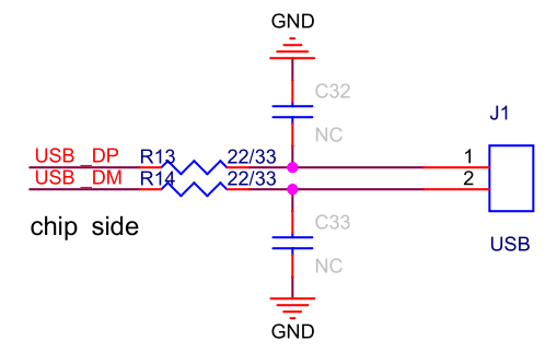
ESP32-C6 USB RC Schematic
Note that upon power-up, the USB_D+ signal will fluctuate between high and low states. The high-level signal is relatively strong and requires a robust pull-down resistor to drive it low. Therefore, if you need a stable initial state, adding an external pull-up resistor is recommended to ensure a consistent high-level output voltage at startup.
ESP32-C6 also supports download functions and log message printing via USB. For details please refer to Section Download Guidelines.