SPI Master driver
Overview
The ESP32 has four SPI peripheral devices, called SPI0, SPI1, HSPI and VSPI. SPI0 is entirely dedicated to the flash cache the ESP32 uses to map the SPI flash device it is connected to into memory. SPI1 is connected to the same hardware lines as SPI0 and is used to write to the flash chip. HSPI and VSPI are free to use. SPI1, HSPI and VSPI all have three chip select lines, allowing them to drive up to three SPI devices each as a master.
The spi_master driver
The spi_master driver allows easy communicating with SPI slave devices, even in a multithreaded environment. It fully transparently handles DMA transfers to read and write data and automatically takes care of multiplexing between different SPI slaves on the same master
Terminology
The spi_master driver uses the following terms:
- Host: The SPI peripheral inside the ESP32 initiating the SPI transmissions. One of SPI, HSPI or VSPI. (For now, only HSPI or VSPI are actually supported in the driver; it will support all 3 peripherals somewhere in the future.)
- Bus: The SPI bus, common to all SPI devices connected to one host. In general the bus consists of the
miso, mosi, sclk and optionally quadwp and quadhd signals. The SPI slaves are connected to these
signals in parallel.
- miso - Also known as q, this is the input of the serial stream into the ESP32
- mosi - Also known as d, this is the output of the serial stream from the ESP32
- sclk - Clock signal. Each data bit is clocked out or in on the positive or negative edge of this signal
- quadwp - Write Protect signal. Only used for 4-bit (qio/qout) transactions.
- quadhd - Hold signal. Only used for 4-bit (qio/qout) transactions.
- Device: A SPI slave. Each SPI slave has its own chip select (CS) line, which is made active when a transmission to/from the SPI slave occurs.
- Transaction: One instance of CS going active, data transfer from and/or to a device happening, and CS going inactive again. Transactions are atomic, as in they will never be interrupted by another transaction.
SPI transactions
A transaction on the SPI bus consists of five phases, any of which may be skipped:
- The command phase. In this phase, a command (0-16 bit) is clocked out.
- The address phase. In this phase, an address (0-64 bit) is clocked out.
- The write phase. The master sends data to the slave.
- The dummy phase. The phase is configurable, used to meet the timing requirements.
- The read phase. The slave sends data to the master.
In full duplex mode, the read and write phases are combined, and the SPI host reads and
writes data simultaneously. The total transaction length is decided by
command_bits + address_bits + trans_conf.length, while the trans_conf.rx_length
only determins length of data received into the buffer.
While in half duplex mode, the host have independent write and read phases. The length of write phase and read phase are
decided by trans_conf.length and trans_conf.rx_length respectively.
The command and address phase are optional in that not every SPI device will need to be sent a command
and/or address. This is reflected in the device configuration: when the command_bits or address_bits
fields are set to zero, no command or address phase is done.
Something similar is true for the read and write phase: not every transaction needs both data to be written
as well as data to be read. When rx_buffer is NULL (and SPI_USE_RXDATA) is not set) the read phase
is skipped. When tx_buffer is NULL (and SPI_USE_TXDATA) is not set) the write phase is skipped.
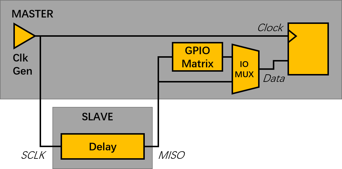
GPIO matrix and IOMUX
Most peripheral signals in ESP32 can connect directly to a specific GPIO, which is called its IOMUX pin. When a peripheral signal is routed to a pin other than its IOMUX pin, ESP32 uses the less direct GPIO matrix to make this connection.
If the driver is configured with all SPI signals set to their specific IOMUX pins (or left unconnected), it will bypass the GPIO matrix. If any SPI signal is configured to a pin other than its IOMUx pin, the driver will automatically route all the signals via the GPIO Matrix. The GPIO matrix samples all signals at 80MHz and sends them between the GPIO and the peripheral.
When the GPIO matrix is used, signals faster than 40MHz cannot propagate and the setup time of MISO is more easily violated, since the input delay of MISO signal is increased. The maximum clock frequency with GPIO Matrix is 40MHz or less, whereas using all IOMUX pins allows 80MHz.
Note
More details about influence of input delay on the maximum clock frequency, see Timing considerations below.
IOMUX pins for SPI controllers are as below:
| Pin Name | HSPI | VSPI |
|---|---|---|
| GPIO Number | ||
| CS0* | 15 | 5 |
| SCLK | 14 | 18 |
| MISO | 12 | 19 |
| MOSI | 13 | 23 |
| QUADWP | 2 | 22 |
| QUADHD | 4 | 21 |
note * Only the first device attaching to the bus can use CS0 pin.
Using the spi_master driver
- Initialize a SPI bus by calling
spi_bus_initialize. Make sure to set the correct IO pins in thebus_configstruct. Take care to set signals that are not needed to -1. - Tell the driver about a SPI slave device connected to the bus by calling spi_bus_add_device.
Make sure to configure any timing requirements the device has in the
dev_configstructure. You should now have a handle for the device, to be used when sending it a transaction. - To interact with the device, fill one or more spi_transaction_t structure with any transaction
parameters you need. Either queue all transactions by calling
spi_device_queue_trans, later quering the result usingspi_device_get_trans_result, or handle all requests synchroneously by feeding them intospi_device_transmit. - Optional: to unload the driver for a device, call
spi_bus_remove_devicewith the device handle as an argument - Optional: to remove the driver for a bus, make sure no more drivers are attached and call
spi_bus_free.
Command and address phases
During the command and address phases, cmd and addr field in the
spi_transaction_t struct are sent to the bus, while nothing is read at the
same time. The default length of command and address phase are set in the
spi_device_interface_config_t and by spi_bus_add_device. When the the
flag SPI_TRANS_VARIABLE_CMD and SPI_TRANS_VARIABLE_ADDR are not set in
the spi_transaction_t,the driver automatically set the length of these
phases to the default value as set when the device is initialized respectively.
If the length of command and address phases needs to be variable, declare a
spi_transaction_ext_t descriptor, set the flag SPI_TRANS_VARIABLE_CMD
or/and SPI_TRANS_VARIABLE_ADDR in the flags of base member and
configure the rest part of base as usual. Then the length of each phases
will be command_bits and address_bits set in the spi_transaction_ext_t.
Write and read phases
Normally, data to be transferred to or from a device will be read from or written to a chunk of memory
indicated by the rx_buffer and tx_buffer members of the transaction structure.
When DMA is enabled for transfers, these buffers are highly recommended to meet the requirements as below:
- allocated in DMA-capable memory using
pvPortMallocCaps(size, MALLOC_CAP_DMA);- 32-bit aligned (start from the boundary and have length of multiples of 4 bytes).
If these requirements are not satisfied, efficiency of the transaction will suffer due to the allocation and memcpy of temporary buffers.
Note
Half duplex transactions with both read and write phases are not supported when using DMA. See Known Issues for details and workarounds.
Sometimes, the amount of data is very small making it less than optimal allocating a separate buffer
for it. If the data to be transferred is 32 bits or less, it can be stored in the transaction struct
itself. For transmitted data, use the tx_data member for this and set the SPI_USE_TXDATA flag
on the transmission. For received data, use rx_data and set SPI_USE_RXDATA. In both cases, do
not touch the tx_buffer or rx_buffer members, because they use the same memory locations
as tx_data and rx_data.
Speed and Timing Considerations
Transferring speed
There’re three factors limiting the transferring speed: (1) The transaction interval, (2) The SPI clock frequency used. (3) The cache miss of SPI functions including callbacks. When large transactions are used, the clock frequency determines the transferring speed; while the interval effects the speed a lot if small transactions are used.
Transaction interval: The interval mainly comes from the cost of FreeRTOS queues and the time switching between tasks and the ISR. It also takes time for the software to setup spi peripheral registers as well as copy data to FIFOs, or setup DMA links. Depending on whether the DMA is used, the interval of an one-byte transaction is around 25us typically.
- The CPU is blocked and switched to other tasks when the transaction is in flight. This save the cpu time but increase the interval.
- When the DMA is enabled, it needs about 2us per transaction to setup the linked list. When the master is transferring, it automatically read data from the linked list. If the DMA is not enabled, CPU has to write/read each byte to/from the FIFO by itself. Usually this is faster than 2us, but the transaction length is limited to 32 bytes for both write and read.
Typical transaction interval with one byte data is as below:
Transaction Time Typical (us) DMA 24 No DMA 22 SPI clock frequency: Each byte transferred takes 8 times of the clock period 8/fspi. If the clock frequency is too high, some functions may be limited to use. See Timing considerations.
The cache miss: the default config puts only the ISR into the IRAM. Other SPI related functions including the driver itself and the callback may suffer from the cache miss and wait for some time while reading code from the flash. Select
CONFIG_SPI_MASTER_IN_IRAMto put the whole SPI driver into IRAM, and put the entire callback(s) and its callee functions into IRAM to prevent this.
For a normal transaction, the overall cost is 20+8n/Fspi[MHz] [us] for n bytes tranferred in one transaction. Hence the transferring speed is : n/(20+8n/Fspi). Example of transferring speed under 8MHz clock speed:
Frequency (MHz) |
Transaction Interval (us) |
Transaction Length (bytes) |
Total Time (us) |
Total Speed (kBps) |
|---|---|---|---|---|
| 8 | 25 | 1 | 26 | 38.5 |
| 8 | 25 | 8 | 33 | 242.4 |
| 8 | 25 | 16 | 41 | 490.2 |
| 8 | 25 | 64 | 89 | 719.1 |
| 8 | 25 | 128 | 153 | 836.6 |
When the length of transaction is short, the cost of transaction interval is really high. Please try to squash data into one transaction if possible to get higher transfer speed.
BTW, the ISR is disabled during flash operation by default. To keep sending
transactions during flash operations, enable
CONFIG_SPI_MASTER_ISR_IN_IRAM and set ESP_INTR_FLAG_IRAM
in the intr_flags member of spi_bus_config_t. Then all the
transactions queued before the flash operations will be handled by the ISR
continuously during flash operation. Note that the callback of each devices,
and their callee functions, should be in the IRAM in this case, or your
callback will crash due to cache miss.
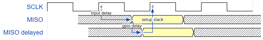
Timing considerations
As shown in the figure below, there is a delay on the MISO signal after SCLK launch edge and before it’s latched by the internal register. As a result, the MISO pin setup time is the limiting factor for SPI clock speed. When the delay is too large, setup slack is < 0 and the setup timing requirement is violated, leads to the failure of reading correctly.
The maximum frequency allowed is related to the input delay (maximum valid
time after SCLK on the MISO bus), as well as the usage of GPIO matrix. The
maximum frequency allowed is reduced to about 33~77% (related to existing
input delay) when the GPIO matrix is used. To work at higher frequency, you
have to use the IOMUX pins or the dummy bit workaround. You can get the
maximum reading frequency of the master by spi_get_freq_limit.
Dummy bit workaround: We can insert dummy clocks (during which the host does not read data) before the read phase actually begins. The slave still sees the dummy clocks and gives out data, but the host does not read until the read phase. This compensates the lack of setup time of MISO required by the host, allowing the host reading at higher frequency.
In the ideal case (the slave is so fast that the input delay is shorter than an apb clock, 12.5ns), the maximum frequency host can read (or read and write) under different conditions is as below:
| Frequency Limit (MHz) | Dummy Bits Used By Driver | Comments | |
|---|---|---|---|
| GPIO matrix | IOMUX pins | ||
| 26.6 | 80 | No | |
| 40 | – | Yes | Half Duplex, no DMA allowed |
And if the host only writes, the dummy bit workaround is not used and the frequency limit is as below:
| GPIO matrix (MHz) | IOMUX pins (MHz) |
|---|---|
| 40 | 80 |
The spi master driver can work even if the input delay in the spi_device_interface_config_t is set to 0.
However, setting a accurate value helps to: (1) calculate the frequency limit in full duplex mode, and (2) compensate
the timing correctly by dummy bits in half duplex mode. You may find the maximum data valid time after the launch edge
of SPI clocks in the AC characteristics chapter of the device specifications, or measure the time on a oscilloscope or
logic analyzer.
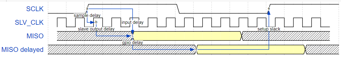
As shown in the figure above, the input delay is usually:
[input delay] = [sample delay] + [slave output delay]
- The sample delay is the maximum random delay due to the asynchronization of SCLK and peripheral clock of the slave. It’s usually 1 slave peripheral clock if the clock is asynchronize with SCLK, or 0 if the slave just use the SCLK to latch the SCLK and launch MISO data. e.g. for ESP32 slaves, the delay is 12.5ns (1 apb clock), while it is reduced to 0 if the slave is in the same chip as the master.
- The slave output delay is the time for the MOSI to be stable after the launch edge. e.g. for ESP32 slaves, the output delay is 37.5ns (3 apb clocks) when IOMUX pins in the slave is used, or 62.5ns (5 apb clocks) if through the GPIO matrix.
Some typical delays are shown in the following table:
| Device | Input delay (ns) |
|---|---|
| Ideal device | 0 |
| ESP32 slave IOMUX* | 50 |
| ESP32 slave GPIO* | 75 |
| ESP32 slave is on an independent chip, 12.5ns sample delay included. | |
The MISO path delay(tv), consists of slave input delay and master GPIO matrix delay, finally determines the frequency limit, above which the full duplex mode will not work, or dummy bits are used in the half duplex mode. The frequency limit is:
Freq limit[MHz] = 80 / (floor(MISO delay[ns]/12.5) + 1)
The figure below shows the relations of frequency limit against the input delay. 2 extra apb clocks should be counted into the MISO delay if the GPIO matrix in the master is used.
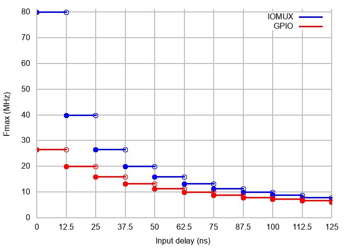
Corresponding frequency limit for different devices with different input delay are shown in the following table:
| Master | Input delay (ns) | MISO path delay (ns) | Freq. limit (MHz) |
|---|---|---|---|
| IOMUX (0ns) | 0 | 0 | 80 |
| 50 | 50 | 16 | |
| 75 | 75 | 11.43 | |
| GPIO (25ns) | 0 | 25 | 26.67 |
| 50 | 75 | 11.43 | |
| 75 | 100 | 8.89 |
Thread Safety
The SPI driver API is thread safe when multiple SPI devices on the same bus are accessed from different tasks. However, the driver is not thread safe if the same SPI device is accessed from multiple tasks.
In this case, it is recommended to either refactor your application so only a single task accesses each SPI device, or to add mutex locking around access of the shared device.
Known Issues
Half duplex mode is not compatible with DMA when both writing and reading phases exist.
If such transactions are required, you have to use one of the alternative solutions:
use full-duplex mode instead.
disable the DMA by setting the last parameter to 0 in bus initialization function just as below:
ret=spi_bus_initialize(VSPI_HOST, &buscfg, 0);this may prohibit you from transmitting and receiving data longer than 32 bytes.
try to use command and address field to replace the write phase.
Full duplex mode is not compatible with the dummy bit workaround, hence the frequency is limited. See dummy bit speed-up workaround.
Application Example
Display graphics on the 320x240 LCD of WROVER-Kits: peripherals/spi_master.
API Reference - SPI Common
Header File
Functions
-
bool
spicommon_periph_claim(spi_host_device_t host)¶ Try to claim a SPI peripheral.
Call this if your driver wants to manage a SPI peripheral.
- Return
- True if peripheral is claimed successfully; false if peripheral already is claimed.
- Parameters
host: Peripheral to claim
-
bool
spicommon_periph_free(spi_host_device_t host)¶ Return the SPI peripheral so another driver can claim it.
- Return
- True if peripheral is returned successfully; false if peripheral was free to claim already.
- Parameters
host: Peripheral to return
-
bool
spicommon_dma_chan_claim(int dma_chan)¶ Try to claim a SPI DMA channel.
Call this if your driver wants to use SPI with a DMA channnel.
- Return
- True if success; false otherwise.
- Parameters
dma_chan: channel to claim
-
bool
spicommon_dma_chan_free(int dma_chan)¶ Return the SPI DMA channel so other driver can claim it, or just to power down DMA.
- Return
- True if success; false otherwise.
- Parameters
dma_chan: channel to return
-
esp_err_t
spicommon_bus_initialize_io(spi_host_device_t host, const spi_bus_config_t *bus_config, int dma_chan, uint32_t flags, uint32_t *flags_o)¶ Connect a SPI peripheral to GPIO pins.
This routine is used to connect a SPI peripheral to the IO-pads and DMA channel given in the arguments. Depending on the IO-pads requested, the routing is done either using the IO_mux or using the GPIO matrix.
- Return
- ESP_ERR_INVALID_ARG if parameter is invalid
- ESP_OK on success
- Parameters
host: SPI peripheral to be routedbus_config: Pointer to a spi_bus_config struct detailing the GPIO pinsdma_chan: DMA-channel (1 or 2) to use, or 0 for no DMA.flags: Combination of SPICOMMON_BUSFLAG_* flags, set to ensure the pins set are capable with some functions:SPICOMMON_BUSFLAG_MASTER: Initialize I/O in master modeSPICOMMON_BUSFLAG_SLAVE: Initialize I/O in slave modeSPICOMMON_BUSFLAG_NATIVE_PINS: Pins set should match the iomux pins of the controller.SPICOMMON_BUSFLAG_SCLK,SPICOMMON_BUSFLAG_MISO,SPICOMMON_BUSFLAG_MOSI: Make sure SCLK/MISO/MOSI is/are set to a valid GPIO. Also check output capability according to the mode.SPICOMMON_BUSFLAG_DUAL: Make sure both MISO and MOSI are output capable so that DIO mode is capable.SPICOMMON_BUSFLAG_WPHDMake sure WP and HD are set to valid output GPIOs.SPICOMMON_BUSFLAG_QUAD: Combination ofSPICOMMON_BUSFLAG_DUALandSPICOMMON_BUSFLAG_WPHD.
flags_o: A SPICOMMON_BUSFLAG_* flag combination of bus abilities will be written to this address. Leave to NULL if not needed.SPICOMMON_BUSFLAG_NATIVE_PINS: The bus is connected to iomux pins.SPICOMMON_BUSFLAG_SCLK,SPICOMMON_BUSFLAG_MISO,SPICOMMON_BUSFLAG_MOSI: The bus has CLK/MISO/MOSI connected.SPICOMMON_BUSFLAG_DUAL: The bus is capable with DIO mode.SPICOMMON_BUSFLAG_WPHDThe bus has WP and HD connected.SPICOMMON_BUSFLAG_QUAD: Combination ofSPICOMMON_BUSFLAG_DUALandSPICOMMON_BUSFLAG_WPHD.
-
esp_err_t
spicommon_bus_free_io(spi_host_device_t host)¶ Free the IO used by a SPI peripheral.
- Return
- ESP_ERR_INVALID_ARG if parameter is invalid
- ESP_OK on success
- Parameters
host: SPI peripheral to be freed
-
esp_err_t
spicommon_bus_free_io_cfg(const spi_bus_config_t *bus_cfg)¶ Free the IO used by a SPI peripheral.
- Return
- ESP_ERR_INVALID_ARG if parameter is invalid
- ESP_OK on success
- Parameters
bus_cfg: Bus config struct which defines which pins to be used.
-
void
spicommon_cs_initialize(spi_host_device_t host, int cs_io_num, int cs_num, int force_gpio_matrix)¶ Initialize a Chip Select pin for a specific SPI peripheral.
- Parameters
host: SPI peripheralcs_io_num: GPIO pin to routecs_num: CS id to routeforce_gpio_matrix: If true, CS will always be routed through the GPIO matrix. If false, if the GPIO number allows it, the routing will happen through the IO_mux.
-
void
spicommon_cs_free(spi_host_device_t host, int cs_num)¶ Free a chip select line.
- Parameters
host: SPI peripheralcs_num: CS id to free
-
void
spicommon_cs_free_io(int cs_gpio_num)¶ Free a chip select line.
- Parameters
cs_gpio_num: CS gpio num to free
-
void
spicommon_setup_dma_desc_links(lldesc_t *dmadesc, int len, const uint8_t *data, bool isrx)¶ Setup a DMA link chain.
This routine will set up a chain of linked DMA descriptors in the array pointed to by
dmadesc. Enough DMA descriptors will be used to fit the buffer oflenbytes in, and the descriptors will point to the corresponding positions inbufferand linked together. The end result is that feedingdmadesc[0]into DMA hardware results in the entiretylenbytes ofdatabeing read or written.- Parameters
dmadesc: Pointer to array of DMA descriptors big enough to be able to conveylenbyteslen: Length of bufferdata: Data buffer to use for DMA transferisrx: True if data is to be written intodata, false if it’s to be read fromdata.
-
spi_dev_t *
spicommon_hw_for_host(spi_host_device_t host)¶ Get the position of the hardware registers for a specific SPI host.
- Return
- A register descriptor stuct pointer, pointed at the hardware registers
- Parameters
host: The SPI host
-
int
spicommon_irqsource_for_host(spi_host_device_t host)¶ Get the IRQ source for a specific SPI host.
- Return
- The hosts IRQ source
- Parameters
host: The SPI host
-
bool
spicommon_dmaworkaround_req_reset(int dmachan, dmaworkaround_cb_t cb, void *arg)¶ Request a reset for a certain DMA channel.
Essentially, when a reset is needed, a driver can request this using spicommon_dmaworkaround_req_reset. This is supposed to be called with an user-supplied function as an argument. If both DMA channels are idle, this call will reset the DMA subsystem and return true. If the other DMA channel is still busy, it will return false; as soon as the other DMA channel is done, however, it will reset the DMA subsystem and call the callback. The callback is then supposed to be used to continue the SPI drivers activity.
- Note
- In some (well-defined) cases in the ESP32 (at least rev v.0 and v.1), a SPI DMA channel will get confused. This can be remedied by resetting the SPI DMA hardware in case this happens. Unfortunately, the reset knob used for thsi will reset both DMA channels, and as such can only done safely when both DMA channels are idle. These functions coordinate this.
- Return
- True when a DMA reset could be executed immediately. False when it could not; in this case the callback will be called with the specified argument when the logic can execute a reset, after that reset.
- Parameters
dmachan: DMA channel associated with the SPI host that needs a resetcb: Callback to call in case DMA channel cannot be reset immediatelyarg: Argument to the callback
-
bool
spicommon_dmaworkaround_reset_in_progress()¶ Check if a DMA reset is requested but has not completed yet.
- Return
- True when a DMA reset is requested but hasn’t completed yet. False otherwise.
-
void
spicommon_dmaworkaround_idle(int dmachan)¶ Mark a DMA channel as idle.
A call to this function tells the workaround logic that this channel will not be affected by a global SPI DMA reset.
-
void
spicommon_dmaworkaround_transfer_active(int dmachan)¶ Mark a DMA channel as active.
A call to this function tells the workaround logic that this channel will be affected by a global SPI DMA reset, and a reset like that should not be attempted.
Structures
-
struct
spi_bus_config_t¶ This is a configuration structure for a SPI bus.
You can use this structure to specify the GPIO pins of the bus. Normally, the driver will use the GPIO matrix to route the signals. An exception is made when all signals either can be routed through the IO_MUX or are -1. In that case, the IO_MUX is used, allowing for >40MHz speeds.
- Note
- Be advised that the slave driver does not use the quadwp/quadhd lines and fields in spi_bus_config_t refering to these lines will be ignored and can thus safely be left uninitialized.
Public Members
-
int
mosi_io_num¶ GPIO pin for Master Out Slave In (=spi_d) signal, or -1 if not used.
-
int
miso_io_num¶ GPIO pin for Master In Slave Out (=spi_q) signal, or -1 if not used.
-
int
sclk_io_num¶ GPIO pin for Spi CLocK signal, or -1 if not used.
-
int
quadwp_io_num¶ GPIO pin for WP (Write Protect) signal which is used as D2 in 4-bit communication modes, or -1 if not used.
-
int
quadhd_io_num¶ GPIO pin for HD (HolD) signal which is used as D3 in 4-bit communication modes, or -1 if not used.
-
int
max_transfer_sz¶ Maximum transfer size, in bytes. Defaults to 4094 if 0.
-
uint32_t
flags¶ Abilities of bus to be checked by the driver. Or-ed value of
SPICOMMON_BUSFLAG_*flags.
-
int
intr_flags¶ Interrupt flag for the bus to set the priority, and IRAM attribute, see
esp_intr_alloc.h. Note that the EDGE, INTRDISABLED attribute are ignored by the driver. Note that if ESP_INTR_FLAG_IRAM is set, ALL the callbacks of the driver, and their callee functions, should be put in the IRAM.
Macros
-
SPI_MAX_DMA_LEN
-
SPICOMMON_BUSFLAG_SLAVE¶ Initialize I/O in slave mode.
-
SPICOMMON_BUSFLAG_MASTER¶ Initialize I/O in master mode.
-
SPICOMMON_BUSFLAG_NATIVE_PINS¶ Check using iomux pins. Or indicates the pins are configured through the IO mux rather than GPIO matrix.
-
SPICOMMON_BUSFLAG_SCLK¶ Check existing of SCLK pin. Or indicates CLK line initialized.
-
SPICOMMON_BUSFLAG_MISO¶ Check existing of MISO pin. Or indicates MISO line initialized.
-
SPICOMMON_BUSFLAG_MOSI¶ Check existing of MOSI pin. Or indicates CLK line initialized.
-
SPICOMMON_BUSFLAG_DUAL¶ Check MOSI and MISO pins can output. Or indicates bus able to work under DIO mode.
-
SPICOMMON_BUSFLAG_WPHD¶ Check existing of WP and HD pins. Or indicates WP & HD pins initialized.
-
SPICOMMON_BUSFLAG_QUAD¶ Check existing of MOSI/MISO/WP/HD pins as output. Or indicates bus able to work under QIO mode.
API Reference - SPI Master
Header File
Functions
-
esp_err_t
spi_bus_initialize(spi_host_device_t host, const spi_bus_config_t *bus_config, int dma_chan)¶ Initialize a SPI bus.
- Warning
- For now, only supports HSPI and VSPI.
- Warning
- If a DMA channel is selected, any transmit and receive buffer used should be allocated in DMA-capable memory.
- Return
- ESP_ERR_INVALID_ARG if configuration is invalid
- ESP_ERR_INVALID_STATE if host already is in use
- ESP_ERR_NO_MEM if out of memory
- ESP_OK on success
- Parameters
host: SPI peripheral that controls this busbus_config: Pointer to a spi_bus_config_t struct specifying how the host should be initializeddma_chan: Either channel 1 or 2, or 0 in the case when no DMA is required. Selecting a DMA channel for a SPI bus allows transfers on the bus to have sizes only limited by the amount of internal memory. Selecting no DMA channel (by passing the value 0) limits the amount of bytes transfered to a maximum of 32.
-
esp_err_t
spi_bus_free(spi_host_device_t host)¶ Free a SPI bus.
- Warning
- In order for this to succeed, all devices have to be removed first.
- Return
- ESP_ERR_INVALID_ARG if parameter is invalid
- ESP_ERR_INVALID_STATE if not all devices on the bus are freed
- ESP_OK on success
- Parameters
host: SPI peripheral to free
-
esp_err_t
spi_bus_add_device(spi_host_device_t host, const spi_device_interface_config_t *dev_config, spi_device_handle_t *handle)¶ Allocate a device on a SPI bus.
This initializes the internal structures for a device, plus allocates a CS pin on the indicated SPI master peripheral and routes it to the indicated GPIO. All SPI master devices have three CS pins and can thus control up to three devices.
- Note
- While in general, speeds up to 80MHz on the dedicated SPI pins and 40MHz on GPIO-matrix-routed pins are supported, full-duplex transfers routed over the GPIO matrix only support speeds up to 26MHz.
- Return
- ESP_ERR_INVALID_ARG if parameter is invalid
- ESP_ERR_NOT_FOUND if host doesn’t have any free CS slots
- ESP_ERR_NO_MEM if out of memory
- ESP_OK on success
- Parameters
host: SPI peripheral to allocate device ondev_config: SPI interface protocol config for the devicehandle: Pointer to variable to hold the device handle
-
esp_err_t
spi_bus_remove_device(spi_device_handle_t handle)¶ Remove a device from the SPI bus.
- Return
- ESP_ERR_INVALID_ARG if parameter is invalid
- ESP_ERR_INVALID_STATE if device already is freed
- ESP_OK on success
- Parameters
handle: Device handle to free
-
esp_err_t
spi_device_queue_trans(spi_device_handle_t handle, spi_transaction_t *trans_desc, TickType_t ticks_to_wait)¶ Queue a SPI transaction for execution.
- Return
- ESP_ERR_INVALID_ARG if parameter is invalid
- ESP_ERR_TIMEOUT if there was no room in the queue before ticks_to_wait expired
- ESP_ERR_NO_MEM if allocating DMA-capable temporary buffer failed
- ESP_OK on success
- Parameters
handle: Device handle obtained using spi_host_add_devtrans_desc: Description of transaction to executeticks_to_wait: Ticks to wait until there’s room in the queue; use portMAX_DELAY to never time out.
-
esp_err_t
spi_device_get_trans_result(spi_device_handle_t handle, spi_transaction_t **trans_desc, TickType_t ticks_to_wait)¶ Get the result of a SPI transaction queued earlier.
This routine will wait until a transaction to the given device (queued earlier with spi_device_queue_trans) has succesfully completed. It will then return the description of the completed transaction so software can inspect the result and e.g. free the memory or re-use the buffers.
- Return
- ESP_ERR_INVALID_ARG if parameter is invalid
- ESP_ERR_TIMEOUT if there was no completed transaction before ticks_to_wait expired
- ESP_OK on success
- Parameters
handle: Device handle obtained using spi_host_add_devtrans_desc: Pointer to variable able to contain a pointer to the description of the transaction that is executed. The descriptor should not be modified until the descriptor is returned by spi_device_get_trans_result.ticks_to_wait: Ticks to wait until there’s a returned item; use portMAX_DELAY to never time out.
-
esp_err_t
spi_device_transmit(spi_device_handle_t handle, spi_transaction_t *trans_desc)¶ Send a SPI transaction, wait for it to complete, and return the result.
This function is the equivalent of calling spi_device_queue_trans() followed by spi_device_get_trans_result(). Do not use this when there is still a transaction separately queued from spi_device_queue_trans() that hasn’t been finalized using spi_device_get_trans_result().
- Note
- This function is not thread safe when multiple tasks access the same SPI device.
- Return
- ESP_ERR_INVALID_ARG if parameter is invalid
- ESP_OK on success
- Parameters
handle: Device handle obtained using spi_host_add_devtrans_desc: Description of transaction to execute
-
int
spi_cal_clock(int fapb, int hz, int duty_cycle, uint32_t *reg_o)¶ Calculate the working frequency that is most close to desired frequency, and also the register value.
- Return
- Actual working frequency that most fit.
- Parameters
fapb: The frequency of apb clock, should beAPB_CLK_FREQ.hz: Desired working frequencyduty_cycle: Duty cycle of the spi clockreg_o: Output of value to be set in clock register, or NULL if not needed.
-
void
spi_get_timing(bool gpio_is_used, int input_delay_ns, int eff_clk, int *dummy_o, int *cycles_remain_o)¶ Calculate the timing settings of specified frequency and settings.
- Note
- If **dummy_o* is not zero, it means dummy bits should be applied in half duplex mode, and full duplex mode may not work.
- Parameters
gpio_is_used: True if using GPIO matrix, or False if iomux pins are used.input_delay_ns: Input delay from SCLK launch edge to MISO data valid.eff_clk: Effective clock frequency (in Hz) from spi_cal_clock.dummy_o: Address of dummy bits used output. Set to NULL if not needed.cycles_remain_o: Address of cycles remaining (after dummy bits are used) output.- -1 If too many cycles remaining, suggest to compensate half a clock.
- 0 If no remaining cycles or dummy bits are not used.
- positive value: cycles suggest to compensate.
-
int
spi_get_freq_limit(bool gpio_is_used, int input_delay_ns)¶ Get the frequency limit of current configurations. SPI master working at this limit is OK, while above the limit, full duplex mode and DMA will not work, and dummy bits will be aplied in the half duplex mode.
- Return
- Frequency limit of current configurations.
- Parameters
gpio_is_used: True if using GPIO matrix, or False if native pins are used.input_delay_ns: Input delay from SCLK launch edge to MISO data valid.
Structures
-
struct
spi_device_interface_config_t¶ This is a configuration for a SPI slave device that is connected to one of the SPI buses.
Public Members
-
uint8_t
command_bits¶ Default amount of bits in command phase (0-16), used when
SPI_TRANS_VARIABLE_CMDis not used, otherwise ignored.
-
uint8_t
address_bits¶ Default amount of bits in address phase (0-64), used when
SPI_TRANS_VARIABLE_ADDRis not used, otherwise ignored.
-
uint8_t
dummy_bits¶ Amount of dummy bits to insert between address and data phase.
-
uint8_t
mode¶ SPI mode (0-3)
-
uint8_t
duty_cycle_pos¶ Duty cycle of positive clock, in 1/256th increments (128 = 50%/50% duty). Setting this to 0 (=not setting it) is equivalent to setting this to 128.
-
uint8_t
cs_ena_pretrans¶ Amount of SPI bit-cycles the cs should be activated before the transmission (0-16). This only works on half-duplex transactions.
-
uint8_t
cs_ena_posttrans¶ Amount of SPI bit-cycles the cs should stay active after the transmission (0-16)
-
int
clock_speed_hz¶ Clock speed, divisors of 80MHz, in Hz. See
SPI_MASTER_FREQ_*.
-
int
input_delay_ns¶ Maximum data valid time of slave. The time required between SCLK and MISO valid, including the possible clock delay from slave to master. The driver uses this value to give an extra delay before the MISO is ready on the line. Leave at 0 unless you know you need a delay. For better timing performance at high frequency (over 8MHz), it’s suggest to have the right value.
-
int
spics_io_num¶ CS GPIO pin for this device, or -1 if not used.
-
uint32_t
flags¶ Bitwise OR of SPI_DEVICE_* flags.
-
int
queue_size¶ Transaction queue size. This sets how many transactions can be ‘in the air’ (queued using spi_device_queue_trans but not yet finished using spi_device_get_trans_result) at the same time.
-
transaction_cb_t
pre_cb¶ Callback to be called before a transmission is started.
This callback is called within interrupt context should be in IRAM for best performance, see “Transferring Speed” section in the SPI Master documentation for full details. If not, the callback may crash during flash operation when the driver is initialized with ESP_INTR_FLAG_IRAM.
-
transaction_cb_t
post_cb¶ Callback to be called after a transmission has completed.
This callback is called within interrupt context should be in IRAM for best performance, see “Transferring Speed” section in the SPI Master documentation for full details. If not, the callback may crash during flash operation when the driver is initialized with ESP_INTR_FLAG_IRAM.
-
uint8_t
-
struct
spi_transaction_t¶ This structure describes one SPI transaction. The descriptor should not be modified until the transaction finishes.
Public Members
-
uint32_t
flags¶ Bitwise OR of SPI_TRANS_* flags.
-
uint16_t
cmd¶ Command data, of which the length is set in the
command_bitsof spi_device_interface_config_t.NOTE: this field, used to be “command” in ESP-IDF 2.1 and before, is re-written to be used in a new way in ESP-IDF 3.0.
Example: write 0x0123 and command_bits=12 to send command 0x12, 0x3_ (in previous version, you may have to write 0x3_12).
-
uint64_t
addr¶ Address data, of which the length is set in the
address_bitsof spi_device_interface_config_t.NOTE: this field, used to be “address” in ESP-IDF 2.1 and before, is re-written to be used in a new way in ESP-IDF3.0.
Example: write 0x123400 and address_bits=24 to send address of 0x12, 0x34, 0x00 (in previous version, you may have to write 0x12340000).
-
size_t
length¶ Total data length, in bits.
-
size_t
rxlength¶ Total data length received, should be not greater than
lengthin full-duplex mode (0 defaults this to the value oflength).
-
void *
user¶ User-defined variable. Can be used to store eg transaction ID.
-
const void *
tx_buffer¶ Pointer to transmit buffer, or NULL for no MOSI phase.
-
uint8_t
tx_data[4]¶ If SPI_USE_TXDATA is set, data set here is sent directly from this variable.
-
void *
rx_buffer¶ Pointer to receive buffer, or NULL for no MISO phase. Written by 4 bytes-unit if DMA is used.
-
uint8_t
rx_data[4]¶ If SPI_USE_RXDATA is set, data is received directly to this variable.
-
uint32_t
-
struct
spi_transaction_ext_t¶ This struct is for SPI transactions which may change their address and command length. Please do set the flags in base to
SPI_TRANS_VARIABLE_CMD_ADRto use the bit length here.Public Members
-
struct spi_transaction_t
base¶ Transaction data, so that pointer to spi_transaction_t can be converted into spi_transaction_ext_t.
-
uint8_t
command_bits¶ The command length in this transaction, in bits.
-
uint8_t
address_bits¶ The address length in this transaction, in bits.
-
struct spi_transaction_t
Macros
-
SPI_MASTER_FREQ_8M¶ SPI master clock is divided by 80MHz apb clock. Below defines are example frequencies, and are accurate. Be free to specify a random frequency, it will be rounded to closest frequency (to macros below if above 8MHz). 8MHz
-
SPI_MASTER_FREQ_9M¶ 8.89MHz
-
SPI_MASTER_FREQ_10M¶ 10MHz
-
SPI_MASTER_FREQ_11M¶ 11.43MHz
-
SPI_MASTER_FREQ_13M¶ 13.33MHz
-
SPI_MASTER_FREQ_16M¶ 16MHz
-
SPI_MASTER_FREQ_20M¶ 20MHz
-
SPI_MASTER_FREQ_26M¶ 26.67MHz
-
SPI_MASTER_FREQ_40M¶ 40MHz
-
SPI_MASTER_FREQ_80M¶ 80MHz
-
SPI_DEVICE_TXBIT_LSBFIRST¶ Transmit command/address/data LSB first instead of the default MSB first.
-
SPI_DEVICE_RXBIT_LSBFIRST¶ Receive data LSB first instead of the default MSB first.
-
SPI_DEVICE_BIT_LSBFIRST¶ Transmit and receive LSB first.
-
SPI_DEVICE_3WIRE¶ Use MOSI (=spid) for both sending and receiving data.
-
SPI_DEVICE_POSITIVE_CS¶ Make CS positive during a transaction instead of negative.
-
SPI_DEVICE_HALFDUPLEX¶ Transmit data before receiving it, instead of simultaneously.
-
SPI_DEVICE_CLK_AS_CS¶ Output clock on CS line if CS is active.
-
SPI_DEVICE_NO_DUMMY¶ There are timing issue when reading at high frequency (the frequency is related to whether iomux pins are used, valid time after slave sees the clock).
- In half-duplex mode, the driver automatically inserts dummy bits before reading phase to fix the timing issue. Set this flag to disable this feature.
- In full-duplex mode, however, the hardware cannot use dummy bits, so there is no way to prevent data being read from getting corrupted. Set this flag to confirm that you’re going to work with output only, or read without dummy bits at your own risk.
-
SPI_TRANS_MODE_DIO¶ Transmit/receive data in 2-bit mode.
-
SPI_TRANS_MODE_QIO¶ Transmit/receive data in 4-bit mode.
-
SPI_TRANS_USE_RXDATA¶ Receive into rx_data member of spi_transaction_t instead into memory at rx_buffer.
-
SPI_TRANS_USE_TXDATA¶ Transmit tx_data member of spi_transaction_t instead of data at tx_buffer. Do not set tx_buffer when using this.
-
SPI_TRANS_MODE_DIOQIO_ADDR¶ Also transmit address in mode selected by SPI_MODE_DIO/SPI_MODE_QIO.
-
SPI_TRANS_VARIABLE_CMD¶ Use the
command_bitsinspi_transaction_ext_trather than default value inspi_device_interface_config_t.
-
SPI_TRANS_VARIABLE_ADDR¶ Use the
address_bitsinspi_transaction_ext_trather than default value inspi_device_interface_config_t.
Type Definitions
-
typedef struct spi_transaction_t
spi_transaction_t
-
typedef void (*
transaction_cb_t)(spi_transaction_t *trans)
-
typedef struct spi_device_t *
spi_device_handle_t¶ Handle for a device on a SPI bus.