This chapter introduces the key points of how to design an ESP32-P4 PCB layout using an ESP32-P4 development board as an example.
Considering the communication quality of high-speed signal lines and potential interference with the RF module, please use at least a four-layer PCB design, as follows:
Layer 1 (TOP): Signal traces and components.
Layer 2 (GND): No signal traces here to ensure a complete GND plane.
Layer 3 (POWER): Route power traces here. If possible, route high-speed signal traces here and ensure a complete reference plane.
Whenever possible, route the power traces on the inner layers (not the ground layer) and connect them to the chip pins through vias. Ensure the power traces are surrounded by ground copper.
The trace width for the 3.3 V main power supply should be at least 25 mil.
For the power traces of VDD_LP, VDD_IO_0, VDD_IO_4, VDD_IO_5, VDD_IO_6, VDD_BAT and VDD_ANA, use a trace width of at least 10 mil. Place a 10 µF capacitor at the power entry point for this series of power supply and a 0.1 µF capacitor for each power pin.
The trace width for the main power supply traces of VDD_HP_0, VDD_HP_1, VDD_HP_2, and VDD_HP_3 should be at least 20 mil. Place a 10 µF capacitor at the power entry point for this series of power supply and a 0.1 µF capacitor for each power pin.
For VDD_LDO and VDD_DCDCC, which handle higher current, use a trace width of at least 20 mil and place a 10 µF capacitor close to each power pin.
It is recommended to use a star routing method to distribute power traces to each power pin.
Because the VDD_HP power supply is by default fully controlled internally by ESP32-P4, the external DCDC should be placed close to the chip to ensure that the input, output, and feedback loops are as short as possible.
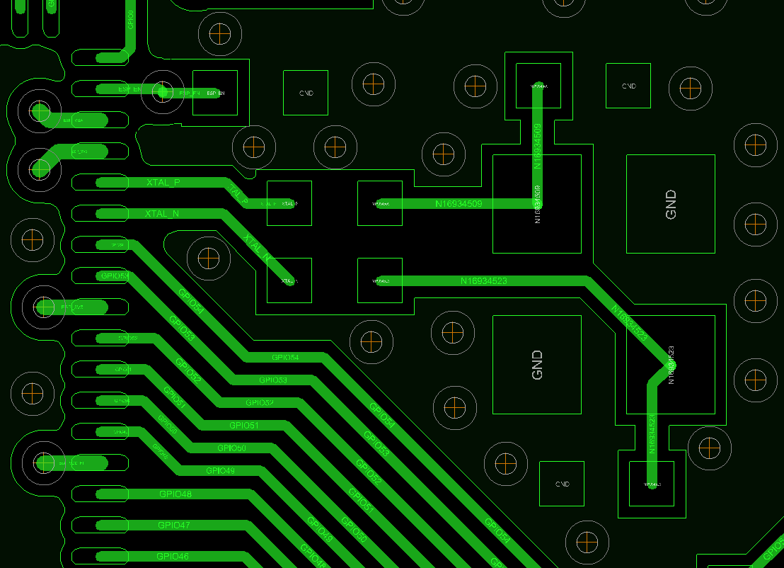
The layout of the crystal should follow the guidelines below:
Ensure a complete GND plane for the crystal and chip.
The crystal should be placed far from the clock pin to avoid interference on the chip. The gap should be at least 4.5 mm. It is good practice to add high-density ground vias stitching around the clock trace for better isolation.
There should be no vias for the clock input and output traces.
Components in series to the crystal trace should be placed close to the chip side.
The external matching capacitors should be placed on the two sides of the crystal, preferably at the end of the clock trace, but not connected directly to the series components. This is to make sure the ground pad of the capacitor is close to that of the crystal.
Do not route high-frequency digital signal traces under the crystal. It is recommended not to route any signal trace under the crystal. The vias on the power traces on both sides of the crystal clock trace should be placed as far away from the clock trace as possible, and the two sides of the clock trace should be surrounded by ground copper.
As the crystal is a sensitive component, do not place any magnetic components nearby that may cause interference, for example large inductance component, and ensure that there is a complete large-area ground plane around the crystal.
The USB layout should meet the following guidelines:
Reserve space for resistors and capacitors on the USB traces close to ESP32-P4.
Use differential pairs with a differential impedance of 90 Ω with a tolerance of ±10%. Use differential pairs and route them in parallel at equal lengths.
USB differential traces should minimize via transitions as much as possible to ensure better impedance control and avoid signal reflections. If vias are necessary, add a pair of ground return vias at each transition point.
Ensure there is a continuous reference layer (a ground layer is recommended) beneath the USB traces.
The SDIO layout should follow the guidelines below:
Minimize parasitic capacitance of SDIO traces as they involve high-speed signals.
The trace lengths for SDIO_CMD and SDIO_DATA0 ~ SDIO_DATA3 should be within ±50 mil of the SDIO_CLK trace length. Use serpentine routing if necessary.
For SDIO routing, maintain a 50 Ω single-ended impedance with a tolerance of ±10%.
Keep the total trace length from SDIO GPIOs to the master SDIO interface as short as possible, ideally within 2000 mil.
Ensure that SDIO traces do not cross layers. Besides, a reference plane (preferably a ground plane) must be placed beneath the traces, and continuity of the reference plane must be ensured.
It is recommended to surround the SDIO_CLK trace with ground copper.
For multi-layer PCB designs, it is recommended to route SDIO traces to an inner layer through vias immediately after being drawn out from the chip. This helps minimize interference with high-speed signal lines. Add a pair of ground return vias at each via transition point.
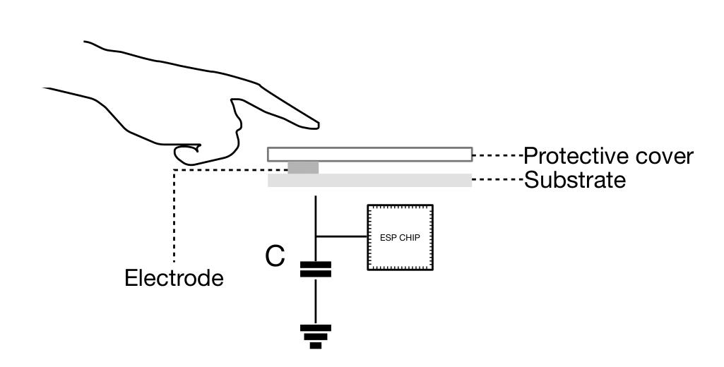
ESP32-P4 offers up to 14 capacitive IOs that detect changes in capacitance on touch sensors due to finger contact or proximity. The chip’s internal capacitance detection circuit features low noise and high sensitivity. It allows to use touch pads with smaller area to implement the touch detection function. You can also use the touch panel array to detect a larger area or more test points.
To prevent capacitive coupling and other electrical interference to the sensitivity of the touch sensor system, the following factors should be taken into account.
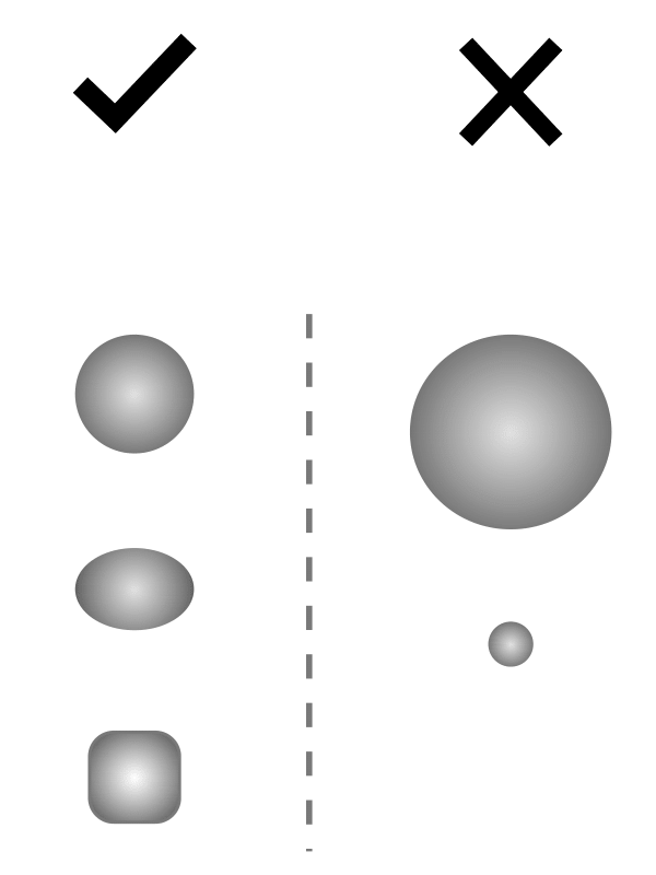
The proper size and shape of an electrode improves system sensitivity. Round, oval, or shapes similar to a human fingertip are commonly applied. Large size or irregular shape might lead to incorrect responses from nearby electrodes.
Figure ESP32-P4 Electrode Pattern Requirements shows the proper and improper size or shape of electrode. Please note that the examples illustrated in the figure are not of actual scale. It is suggested to use a human fingertip as reference.
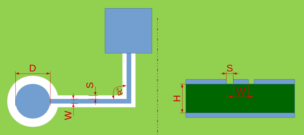
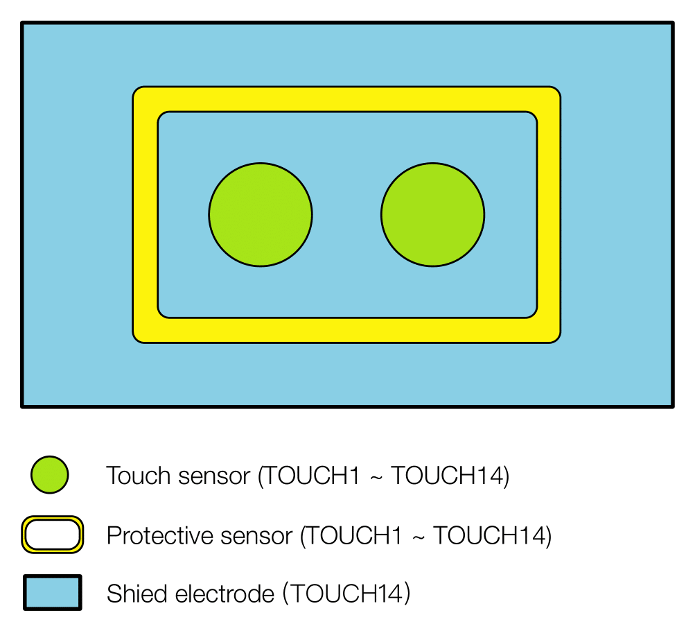
ESP32-P4 touch sensor has a waterproof design and features proximity sensor function. Figure ESP32-P4 Waterproof and Proximity Sensing Design shows an example layout of a waterproof and proximity sensing design.
Note the following guidelines to better implement the waterproof and proximity sensing design:
The recommended width of the shield electrode width is 2 cm.
Employ a grid on the top layer with a trace width of 7 mil and a grid width of 45 mil (25% fill). The filled grid is connected to the driver shield signal.
Employ a grid on the bottom layer with a trace width of 7 mil and a grid width of 70 mil (17% fill). The filled grid is connected to the driver shield signal.
The protective sensor should be in a rectangle shape with curved edges and surround all other sensors.
The recommended width of the protective sensor is 2 mm.
The recommended gap between the protective sensor and shield sensor is 1 mm.
The sensing distance of the proximity sensor is directly proportional to the area of the proximity sensor. However, increasing the sensing area will introduce more noise. Actual testing is needed for optimized performance.
It is recommended that the shape of the proximity sensor is a closed loop. The recommended width is 1.5 mm.
The MIPI layout should follow the guidelines below:
Minimize parasitic capacitance of MIPI traces as they involve high-speed signals.
The impedance of MIPI differential lines should be controlled to 100 Ω, with a tolerance of ±10%.
MIPI traces should be kept equal in length and spacing. The length difference between two MIPI traces in a pair should be minimized and kept within 10 mil; the length difference between different MIPI trace pairs should be minimized and kept within 30 mil. Use serpentine routing if necessary.
It is recommended to surround MIPI trace pairs with ground copper. If this is not feasible, maintain a minimum spacing of 2W between MIPI trace pairs, where “W” is the width of the MIPI trace. For the MIPI CLK trace, surround it with ground copper.
MIPI signal traces should be kept away from other high-speed and high-frequency signals (such as parallel data traces and clock traces) by at least 3W and must not run parallel to them. They should also be kept away from switching power sources and other sources of interference.
Ensure there is a continuous reference layer (preferably a ground layer) below the MIPI signal traces.
For multi-layer PCB designs, it is recommended to route MIPI traces to an inner layer through vias immediately after being drawn out from the chip. This helps minimize interference with high-speed signal lines. Ensure the MIPI CLK traces are surrounded by ground copper. Add a pair of ground return vias at each via transition point.