Schematic Checklist
Overview
The integrated circuitry of ESP32-P4 series chips requires only 40 electrical components (resistors, capacitors, and inductors) and a crystal, as well as an SPI flash and a direct current to direct current converter (DCDC). This chapter details the schematic design of ESP32-P4.
The following figures show the reference schematics of ESP32-P4, which can be used as the basis of your schematic design.
Attention
For new designs, please refer to the schematic of chip revisions v3.0 and later versions.
ESP32-P4 Reference Schematic (Chip Revisions v3.0 and Later)
ESP32-P4 Reference Schematic (Chip Revisions v1.0 and v1.3)
Important
The main differences between chip revisions v1.0/v1.3 (not recommended for new designs) and v3.0 and later versions include the definition of pin 54, the 1 MΩ resistor on the DP pin, the two 499 kΩ resistors and one 22 pF capacitor in the DCDC circuit. For detailed descriptions of these differences, please refer to the following sections.
In chip revisions v3.0 and later versions, pin 54 of ESP32-P4 is defined as VDD_HP_1; in chip revisions v1.0 and v1.3, this pin is defined as NC.
Differences between ESP32-P4 chip revisions and how to distinguish them are described in ESP32-P4 Series SoC Errata.
Any basic ESP32-P4 circuit design includes the following major building blocks:
The rest of this chapter details the specifics of circuit design for each of these sections.
Power Supply
The general recommendations for power supply design are:
For a single power supply, a voltage of 3.3 V is recommended.
The minimum operating supply current of ESP32-P4 is 380 mA (including flash and PSRAM). For the supply current when peripherals are connected, please refer to HP/LP IO Power Supply, MIPI PHY Power Supply and USB PHY Power Supply. Calculate the required supply current based on your application and choose an appropriate power supply chip.
It is suggested to add a 10 μF capacitor at each power entrance.
The power scheme is as shown in Figure ESP32-P4 Power Scheme.
ESP32-P4 Power Scheme
More information about power supply pins can be found in ESP32-P4 Series Datasheet > Section Power Supply.
HP/LP IO Power Supply
Pin No. |
Pin Name |
Direction |
Voltage (V) |
Max. Current (mA) |
IO Pin |
Capacitors (μF) |
|---|---|---|---|---|---|---|
9 |
VDD_LP |
Input |
3.0 ~ 3.6 |
100 |
LP IO |
0.1 |
21 |
VDD_IO_0 |
Input |
1.65 ~ 3.6 |
100 |
HP IO |
0.1 |
62 |
VDD_IO_4 |
Input |
1.65 ~ 3.6 |
100 |
HP IO |
0.1 |
85 |
VDD_IO_5 [1] |
Input |
1.65 ~ 3.6 |
100 |
HP IO |
0.1 |
96 |
VDD_IO_6 |
Input |
1.65 ~ 3.6 |
100 |
HP IO |
0.1 |
MIPI PHY Power Supply
The VDD_MIPI_DPHY of ESP32-P4 is the power supply pin for MIPI PHY. The operating voltage range is 2.25 V ~ 2.75 V. The maximum current consumption is 50 mA. It is recommended to use the internal voltage regulator for power supply, and place 10 nF + 0.1 μF + 1 μF capacitors near VDD_MIPI_DPHY in the circuit.
If the MIPI function is not required, VDD_MIPI_DPHY can be left floating.
Attention
The voltage level of MIPI signals is defined by the MIPI specification. For details, please refer to the relevant MIPI protocol documentation. Note that this is a different concept from the MIPI DPHY voltage level. The 1.8 V/3.3 V levels mentioned in Camera/Display Datasheet refer to signals other than the MIPI signals (Data Lane & CLK), such as MCLK and I2C. The voltage level of MIPI signals is handled internally by the ESP32-P4’s built-in MIPI DPHY and requires no additional configuration.
USB PHY Power Supply
The VDD_USBPHY of ESP32-P4 is the power supply pin for USB PHY. The operating voltage range is 2.97 V ~ 3.63 V. The maximum current consumption is 20 mA. It is recommended to place 10 nF + 0.1 μF + 4.7 μF capacitors near VDD_USBPHY in the circuit.
If DP and DM are not required, the VDD_USBPHY power supply can be left floating.
If DP and DM are required, for chip revisions v1.0 and v1.3 (not recommended for new designs), note that the VDD_USBPHY power supply exhibits leakage current in low power modes. Therefore, it is recommended to add a MOSFET circuit to completely shut off this power supply in low power modes. During the validation phase, a 0 Ω series resistor can be added on VDD_USBPHY.
VDD_USBPHY Reference Schematic (Chip Revisions v1.0 and v1.3)
In chip revisions v3.0 and later versions, this issue has been fixed, and the 0 Ω series resistor can be retained for design compatibility.
Flash and PSRAM IO Power Supply
The VDD_FLASHIO of ESP32-P4 is the power supply pin for FLASH IO. The operating voltage is 1.65 V ~ 3.6 V. This power is supplied by VDDO_FLASH from the voltage regulator. It is recommended to place 0.1 μF + 1 μF capacitors near VDD_FLASHIO in the circuit.
VDD_PSRAM_0 and VDD_PSRAM_1 are power supply pins for PSRAM IO. The operating voltage is 1.65 V ~ 1.95 V. This power is supplied by VDDO_PSRAM from the voltage regulators. It is recommended to place 0.1 μF + 1 μF capacitors near VDD_PSRAM_0 and VDD_PSRAM_1 in the circuit.
Analog Power Supply
The VDD_ANA of ESP32-P4 is an analog power supply pin. The operating voltage range is 3.0 V ~ 3.6 V. It is recommended to place a 0.1 μF capacitor near VDD_ANA in the circuit. The VDD_BAT is also an analog power supply pin. The operating voltage range is 2.5 V ~ 3.6 V. It is recommended to place 0.1 μF + 10 μF capacitors near VDD_BAT.
Pin VDD_BAT must not be left floating. An external battery can be connected. For details, refer to the ESP32-P4 Battery Backup Solution.
Digital Power Supply
VDD_HP_0, VDD_HP_1, VDD_HP_2, and VDD_HP_3 of the ESP32-P4 are digital power supply pins, working in a voltage range of 0.99 V ~ 1.3 V. This power is supplied by ESP_VDD_HP from the external DCDC. It is recommended to place a 10 μF capacitor at the main power source and 0.1 μF capacitors near each power pin.
Internal Voltage Regulators and External DCDC
The VDD_LDO of ESP32-P4 provides power for the low dropout regulators (LDOs). The operating voltage ranges from 3.0 V to 3.6 V. VDD_DCDCC provides power for DCDC. The operating voltage ranges from 3.0 V to 3.6 V. Due to the high current on these pins, place a 10 μF capacitor on the power traces of VDD_LDO and VDD_DCDCC, and add a 0.1 μF capacitor at each pin.
The LDO outputs VDDO_FLASH to power the external flash. The default output is 3.3 V, but it can be configured to 1.8 V by programming EFUSE_0PXA_TIEH_SEL_0.
Note
When using a 1.8 V SPI flash, it is recommended to disconnect the power connection between VDDO_FLASH and the SPI flash until the VDDO_FLASH output voltage has been correctly configured to 1.8 V, to prevent damage to the 1.8 V flash caused by excessive supply voltage.
If this solution is intended for mass production, please contact sales for further support.
Power |
EFUSE_0PXA_TIEH_SEL_0 |
Voltage |
|---|---|---|
flash LDO |
0 |
3.3 V |
2 |
1.8 V |
The LDO outputs VDDO_PSRAM to power the in-package PSRAM. The typical output voltage is 1.9V, which requires software configuration. The default output is 0.
The LDO outputs VDDO_3/4 to power the peripherals. The maximum output current is 50 mA. The output voltage ranges from 0.5V to 2.7V/3.3V, which also requires software configuration. The default output is 0.
For software configuration, please refer to Low Dropout Linear Regulator (LDO).
It is recommended to place a 1 μF capacitor near the VDDO_FLASH, VDDO_PSRAM, and VDDO_3/4 in the circuit.
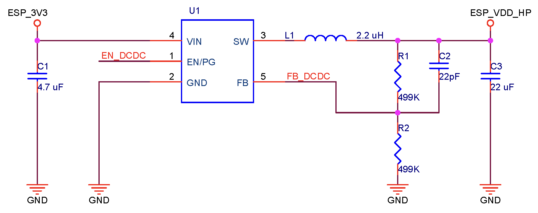
The VDD_HP_0/1/2/3 is powered by an external DC-DC converter (DCDC), with the following details:
The input of the external DCDC is the same as the VDD_DCDCC power supply.
EN_DCDC is the enable pin of the external DCDC. In download mode or when there is no firmware, the voltage on EN_DCDC is 0. After the firmware starts normally, EN_DCDC is controlled internally. In download mode, the EN_DCDC voltage remains at 0. In sleep mode, this pin can be used to disable the power supply to reduce power consumption.
FB_DCDC is the feedback pin of the external DCDC.
EN_DCDC and FB_DCDC pins are fully controlled by the internal circuitry of ESP32-P4 by default. Ensure that they are connected to the EN and FB pins of the external DCDC, respectively, and that the DCDC regulator is placed close to the ESP32-P4. When designing the layout for chip revisions v1.0 and v1.3 (not recommended for new designs), you must reserve pad locations for the feedback resistor and feedback capacitor (components not required). For chip revisions v3.0 and later versions, the feedback resistor and the feedback capacitor must be populated.
Please use verified DCDC models: ETA3485, SY8088, RY3420, BL8028, LP3219, or TLV62569. The input/output specifications and inductor parameters should follow the respective datasheets. Below is the circuit design for TLV62569.
TLV62569 Schematic (Chip Revisions v3.0 and Later)
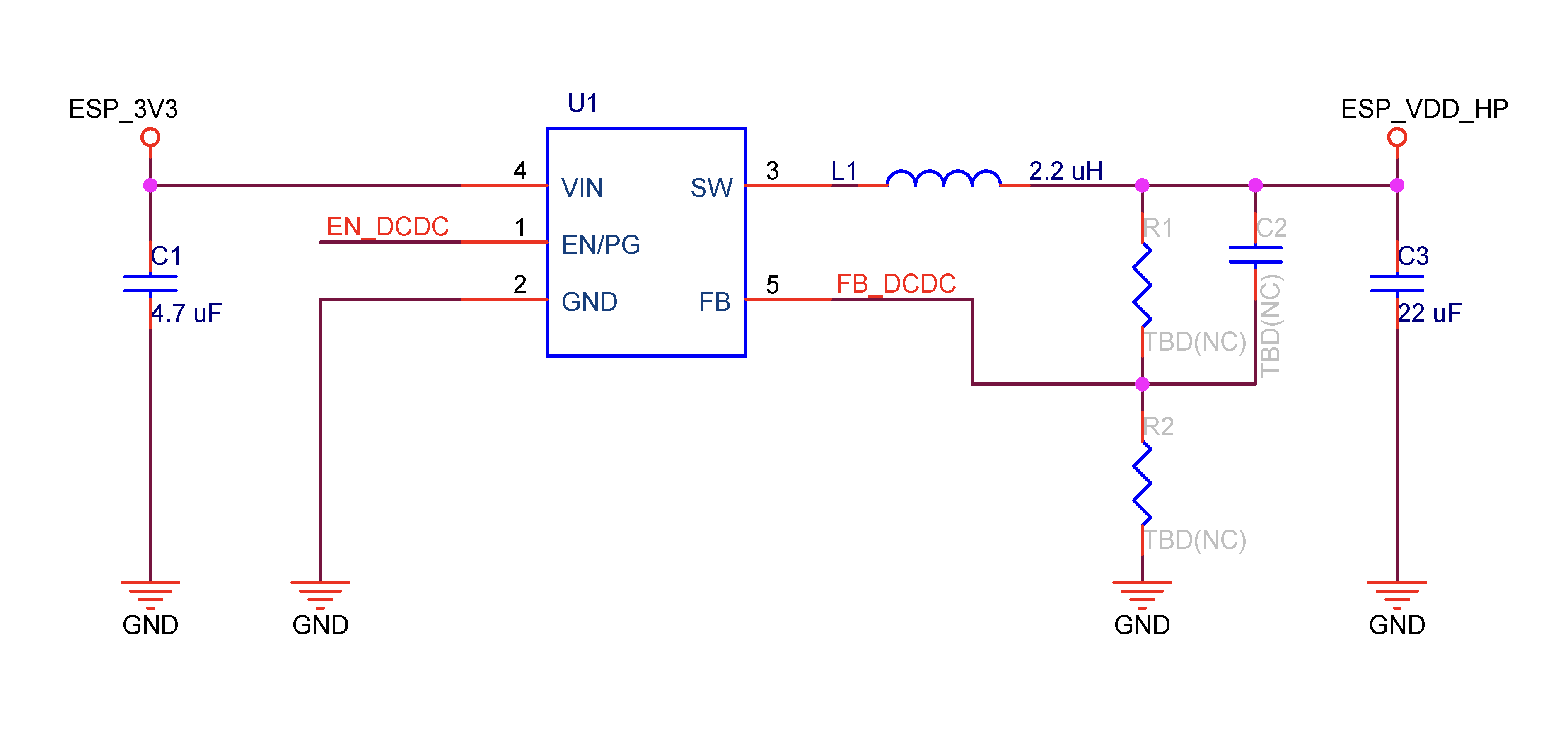
TLV62569 Schematic (Chip Revisions v1.0 and v1.3)
Chip Power-up and Reset Timing
ESP32-P4’s CHIP_PU pin can enable the chip when it is high and reset the chip when it is low.
When ESP32-P4 uses a 3.3 V system power supply, the power rails need some time to stabilize before CHIP_PU is pulled up and the chip is enabled. Therefore, CHIP_PU needs to be asserted high after the 3.3 V rails have been brought up.
To reset the chip, keep the reset voltage VIL_nRST in the range of (–0.3 ~ 0.25 × VDD_BAT) V. To avoid reboots caused by external interferences, make the CHIP_PU trace as short as possible.
Figure ESP32-P4 Power-up and Reset Timing shows the power-up and reset timing of ESP32-P4.
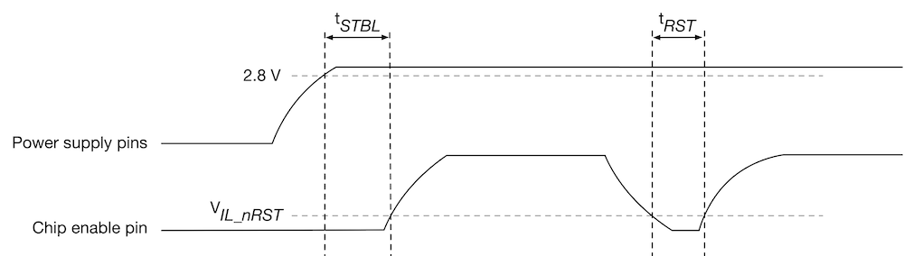
ESP32-P4 Power-up and Reset Timing
Table Description of Timing Parameters for Power-up and Reset provides the specific timing requirements.
Parameter |
Description |
Minimum (µs) |
|---|---|---|
tSTBL |
Time reserved for the power rails to stabilize before the CHIP_PU pin is pulled high to activate the chip |
50 |
tRST |
Time reserved for CHIP_PU to stay below VIL_nRST to reset the chip |
1000 |
Attention
CHIP_PU must not be left floating.
To ensure the correct power-up and reset timing, it is advised to add an RC delay circuit at the CHIP_PU pin. The recommended setting for the RC delay circuit is usually R = 10 kΩ and C = 1 μF. However, specific parameters should be adjusted based on the characteristics of the actual power supply and the power-up and reset timing of the chip.
If the user application has one of the following scenarios:
Slow power rise or fall, such as during battery charging.
Frequent power on/off operations.
Unstable power supply, such as in photovoltaic power generation.
Then, the RC circuit itself may not meet the timing requirements, resulting in the chip being unable to boot correctly. In this case, additional designs need to be added, such as:
Adding an external reset chip or a watchdog chip, typically with a threshold of around 3.0 V.
Implementing reset functionality through a button or the main controller.
Flash and PSRAM
ESP32-P4 requires off-package flash for storing application firmware and data. ESP32-P4 supports up to 64 MB flash, which can be connected via SPI, Dual SPI, and Quad SPI.
ESP32-P4 includes OPI/HPI 1.8 V PSRAM, which is not pinned out externally.
The following table lists the pin mapping between ESP32-P4 and off-package flash for Quad SPI mode. Please note that the pins can connect to one flash at the maximum.
ESP32-P4 |
External Package Flash (Quad SPI) |
|---|---|
FLASH_CK |
CLK |
FLASH_CS |
CS# |
FLASH_D |
DI |
FLASH_Q |
DO |
FLASH_WP |
WP# |
FLASH_HOLD |
HOLD# |
By default, VDDO_FLASH is used as the power supply for flash, and VDDO_PSRAM is used as the power supply for PSRAM.
When VDDO_FLASH is in the output mode of 3.3 V, consider the impact of RVFB on VDD_LDO. For example, when connecting a 3.3 V flash, the following condition must be met:
In the formula above, VDD_flash_min is the minimum operating voltage of the flash, I_flash_max is the maximum operating current of the flash, and RVFB is the on-resistance in 3.3 V mode.
Attention
It is recommended to add zero-ohm resistor footprints in series on the SPI communication lines. These footprints provide flexibility for future adjustments, such as tuning drive strength, mitigating RF interference, correcting signal timing, and reducing noise, if needed.
Place a pull-up resistor at the FLASH_CS pin.
It is recommended to place a 0.1 μF capacitor at the flash power supply pin.
Clock Source
ESP32-P4 supports two external clock sources:
External Crystal Clock Source (Compulsory)
The ESP32-P4 firmware only supports 40 MHz crystal.
The circuit for the crystal is shown in Figure ESP32-P4 Schematic for External Crystal. Note that the accuracy of the selected crystal should be within ±10 ppm.
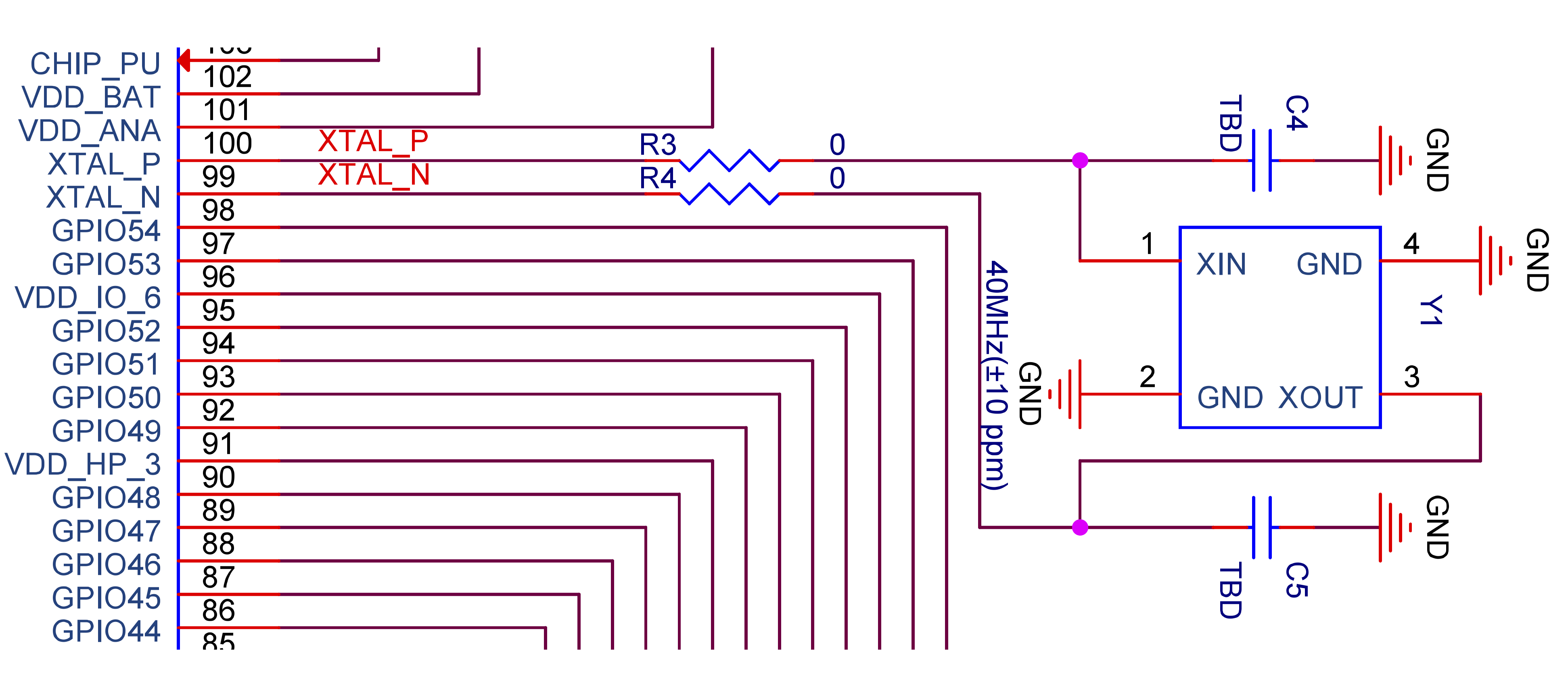
ESP32-P4 Schematic for External Crystal
The initial values of external capacitors C4 and C5 can be determined according to the formula:
In the formula above, the value of CL (load capacitance) can be found in the crystal’s datasheet, and the value of Cstray refers to the PCB’s stray capacitance. The values of C4 and C5 need to be further adjusted after an overall test.
RTC Clock Source (Optional)
ESP32-P4 supports an external 32.768 kHz crystal to act as the RTC clock. The external RTC clock source enhances timing accuracy and consequently decreases average power consumption, without impacting functionality.
Figure ESP32-P4 Schematic for 32.768 kHz Crystal shows the schematic for the external 32.768 kHz crystal.
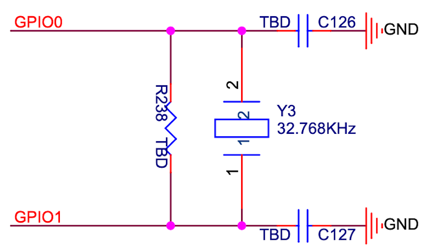
ESP32-P4 Schematic for 32.768 kHz Crystal
Please note the requirements for the 32.768 kHz crystal:
Equivalent series resistance (ESR) ≤ 70 kΩ.
Load capacitance at both ends should be configured according to the crystal’s specification.
The parallel resistor R is used for biasing the crystal circuit (5 MΩ < R ≤ 10 MΩ). In general, you do not need to populate the resistor.
If the RTC clock source is not required, then the pins for the 32.768 kHz crystal can be used as GPIOs.
UART
ESP32-P4 includes five UART interfaces, UART0 ~ UART4, all of which support both hardware flow control (CTS and RTS signals) and software flow control (XON and XOFF). In addition, ESP32-P4 includes one LP UART interface, which also supports both hardware flow control (CTS and RTS signals) and software flow control (XON and XOFF).
The UART0_TXD pin is GPIO37, and the UART0_RXD pin is GPIO38. The other UART0 signals can be mapped to any available GPIO through software configurations. The LP UART TXD is LP GPIO14, and the LP UART RXD is LP GPIO15. The other LP UART signals can be mapped to any available GPIO through software configurations.
Typically, UART0 is used for download and log printing. For instructions on how to download via UART0, please refer to Section Download Guidelines.
It is recommended to use UART1 ~ UART4 as communication serial ports.
SPI
When using the SPI function, to improve EMC performance, add a series resistor (or ferrite bead) and a capacitor to ground on the SPI_CLK trace. If space allows, it is recommended to also add a series resistor and capacitor to ground on other SPI traces. Ensure that the RC/LC components are placed close to the pins of the chip or module.
Strapping Pins
At each startup or reset, a chip requires some initial configuration parameters, such as in which boot mode to load the chip, etc. These parameters are passed over via the strapping pins. After reset, the strapping pins work as normal function pins.
GPIO34, GPIO35, GPIO36, GPIO37, and GPIO38 are strapping pins.
All the information about strapping pins is covered in ESP32-P4 Series Datasheet > Section Boot Configurations. In this document, we will mainly cover the strapping pins related to boot mode.
After chip reset is released, the combination of GPIO35, GPIO36, GPIO37, and GPIO38 controls the boot mode. See Table Chip Boot Mode Control.
Boot Mode |
GPIO35 |
GPIO36 |
GPIO37 |
GPIO38 |
|---|---|---|---|---|
SPI Boot Mode (Default) |
1 |
Any value |
Any value |
Any value |
Joint Download Mode [2] |
0 |
1 |
Any value |
Any value |
Signals applied to the strapping pins should have specific setup time and hold time. For more information, see Figure Setup and Hold Times for Strapping Pins and Table Description of Timing Parameters for Strapping Pins.

Setup and Hold Times for Strapping Pins
Parameter |
Description |
Minimum (ms) |
|---|---|---|
tSU |
Time reserved for the power rails to stabilize before the chip enable pin (CHIP_PU) is pulled high to activate the chip. |
0 |
tH |
Time reserved for the chip to read the strapping pin values after CHIP_PU is already high and before these pins start operating as regular IO pins. |
3 |
Attention
It is recommended to reserve a pull-up resistor at the GPIO35.
Do not add high-value capacitors at GPIO35, otherwise, the chip may enter Joint Download mode instead of SPI Boot mode.
GPIO
The pins of ESP32-P4 can be configured via IO MUX or GPIO matrix. IO MUX provides the default pin configurations (see ESP32-P4 Series Datasheet > Appendix ESP32-P4 Consolidated Pin Overview), whereas the GPIO matrix is used to route signals from peripherals to GPIO pins. For more information about IO MUX and GPIO matrix, please refer to ESP32-P4 Technical Reference Manual > Chapter IO MUX and GPIO Matrix.
Some peripheral signals have already been routed to certain GPIO pins, while some can be routed to any available GPIO pins. For details, please refer to ESP32-P4 Series Datasheet > Section Peripherals.
When using GPIOs, please:
Pay attention to the states of strapping pins during power-up.
Pay attention to the default configurations of the GPIOs after reset. The default configurations can be found in Table IO MUX Pin Functions. It is recommended to add a pull-up or pull-down resistor to pins in the high-impedance state or enable the pull-up and pull-down during software initialization to avoid extra power consumption.
Only GPIOs in the VDD_LP power domain can be controlled in Deep-sleep mode.
When powered solely by the battery, only GPIOs in the VDD_BAT power domain can be controlled.
Pin Number |
Pin Name |
Power Supply Pin |
At Reset |
After Reset |
|---|---|---|---|---|
1 |
GPIO1 |
VDD_LP/VDD_BAT |
– |
– |
2 |
GPIO2 |
VDD_LP/VDD_BAT |
– |
IE, WPU |
3 |
GPIO3 |
VDD_LP/VDD_BAT |
– |
IE |
4 |
GPIO4 |
VDD_LP |
– |
IE |
5 |
GPIO5 |
VDD_LP |
– |
– |
6 |
GPIO6 |
VDD_LP |
– |
– |
7 |
GPIO7 |
VDD_LP |
– |
– |
8 |
GPIO8 |
VDD_LP |
– |
– |
10 |
GPIO9 |
VDD_LP |
– |
– |
11 |
GPIO10 |
VDD_LP |
– |
– |
12 |
GPIO11 |
VDD_LP |
– |
– |
13 |
GPIO12 |
VDD_LP |
– |
– |
14 |
GPIO13 |
VDD_LP |
– |
– |
15 |
GPIO14 |
VDD_LP |
– |
– |
16 |
GPIO15 |
VDD_LP |
– |
– |
17 |
GPIO16 |
VDD_IO_0 |
– |
– |
18 |
GPIO17 |
VDD_IO_0 |
– |
– |
19 |
GPIO18 |
VDD_IO_0 |
– |
– |
20 |
GPIO19 |
VDD_IO_0 |
– |
– |
22 |
GPIO20 |
VDD_IO_0 |
– |
– |
23 |
GPIO21 |
VDD_IO_0 |
– |
– |
24 |
GPIO22 |
VDD_IO_0 |
– |
– |
25 |
GPIO23 |
VDD_IO_0 |
– |
– |
52 |
GPIO24 |
VDD_IO_4 |
– |
– |
53 |
GPIO25 |
VDD_IO_4 |
– |
IE, USB_PU |
55 |
GPIO26 |
VDD_IO_4 |
– |
– |
56 |
GPIO27 |
VDD_IO_4 |
– |
– |
57 |
GPIO28 |
VDD_IO_4 |
– |
– |
58 |
GPIO29 |
VDD_IO_4 |
– |
– |
60 |
GPIO30 |
VDD_IO_4 |
– |
– |
61 |
GPIO31 |
VDD_IO_4 |
– |
– |
63 |
GPIO32 |
VDD_IO_4 |
IE |
– |
64 |
GPIO33 |
VDD_IO_4 |
IE |
– |
65 |
GPIO34 |
VDD_IO_4 |
IE |
– |
66 |
GPIO35 |
VDD_IO_4 |
IE, WPU |
– |
68 |
GPIO36 |
VDD_IO_4 |
IE |
– |
69 |
GPIO37 |
VDD_IO_4 |
IE |
– |
70 |
GPIO38 |
VDD_IO_4 |
IE |
– |
80 |
GPIO39 |
VDD_IO_5 |
– |
– |
81 |
GPIO40 |
VDD_IO_5 |
– |
– |
82 |
GPIO41 |
VDD_IO_5 |
– |
– |
83 |
GPIO42 |
VDD_IO_5 |
– |
– |
84 |
GPIO43 |
VDD_IO_5 |
– |
– |
86 |
GPIO44 |
VDD_IO_5 |
– |
– |
87 |
GPIO45 |
VDD_IO_5 |
– |
– |
88 |
GPIO46 |
VDD_IO_5 |
– |
– |
89 |
GPIO47 |
VDD_IO_5 |
– |
– |
90 |
GPIO48 |
VDD_IO_5 |
– |
– |
92 |
GPIO49 |
VDD_IO_6 |
– |
– |
93 |
GPIO50 |
VDD_IO_6 |
– |
– |
94 |
GPIO51 |
VDD_IO_6 |
– |
– |
95 |
GPIO52 |
VDD_IO_6 |
– |
– |
97 |
GPIO53 |
VDD_IO_6 |
– |
– |
98 |
GPIO54 |
VDD_IO_6 |
– |
– |
104 |
GPIO0 |
VDD_LP/VDD_BAT |
– |
– |
ADC
When using the ADC function, place a 0.1 μF capacitor to ground near the pin to improve accuracy.
ADC Channel Signal |
Pin Name |
|---|---|
ADC1_CHANNEL0 |
GPIO16 |
ADC1_CHANNEL1 |
GPIO17 |
ADC1_CHANNEL2 |
GPIO18 |
ADC1_CHANNEL3 |
GPIO19 |
ADC1_CHANNEL4 |
GPIO20 |
ADC1_CHANNEL5 |
GPIO21 |
ADC1_CHANNEL6 |
GPIO22 |
ADC1_CHANNEL7 |
GPIO23 |
ADC2_CHANNEL0 |
GPIO49 |
ADC2_CHANNEL1 |
GPIO50 |
ADC2_CHANNEL2 |
GPIO51 |
ADC2_CHANNEL3 |
GPIO52 |
ADC2_CHANNEL4 |
GPIO53 |
ADC2_CHANNEL5 |
GPIO54 |
SDIO
ESP32-P4 series chips integrate an SD/MMC host controller, which cannot operate as a slave. The SD/MMC host peripheral provides two slots. Each slot can be used independently to connect to an SD card, SDIO device, or eMMC chip.
Slot 1 (SDMMC_HOST_SLOT_0) signals are fixed to the GPIO pins listed in the table below via the IO MUX and are dedicated to UHS-I mode.
Signal |
Pin Name |
|---|---|
SD1_CDATA0_PAD |
GPIO39 |
SD1_CDATA1_PAD |
GPIO40 |
SD1_CDATA2_PAD |
GPIO41 |
SD1_CDATA3_PAD |
GPIO42 |
SD1_CCLK_PAD |
GPIO43 |
SD1_CCMD_PAD |
GPIO44 |
SD1_CDATA4_PAD |
GPIO45 |
SD1_CDATA5_PAD |
GPIO46 |
SD1_CDATA6_PAD |
GPIO47 |
SD1_CDATA7_PAD |
GPIO48 |
Slot 2 (SDMMC_HOST_SLOT_1) signals can be routed to any GPIO pins through the GPIO matrix, making this slot suitable for non–UHS-I applications.
Please add a pull-up resistor to each SDIO GPIO pin and reserve a series resistor on each SDIO signal line. In addition, reserve a capacitor to ground on the SDIO CLK line for signal tuning.
SDIO 3.0 protocol specifies that the voltage of SDIO GPIOs should switch automatically. Therefore, it is recommended to connect the SDIO GPIO power domain VDD_IO_5 and the external pull-up power supply to VDDO_4. The SD card’s power supply should be connected to the 3.3 V power supply of the system.
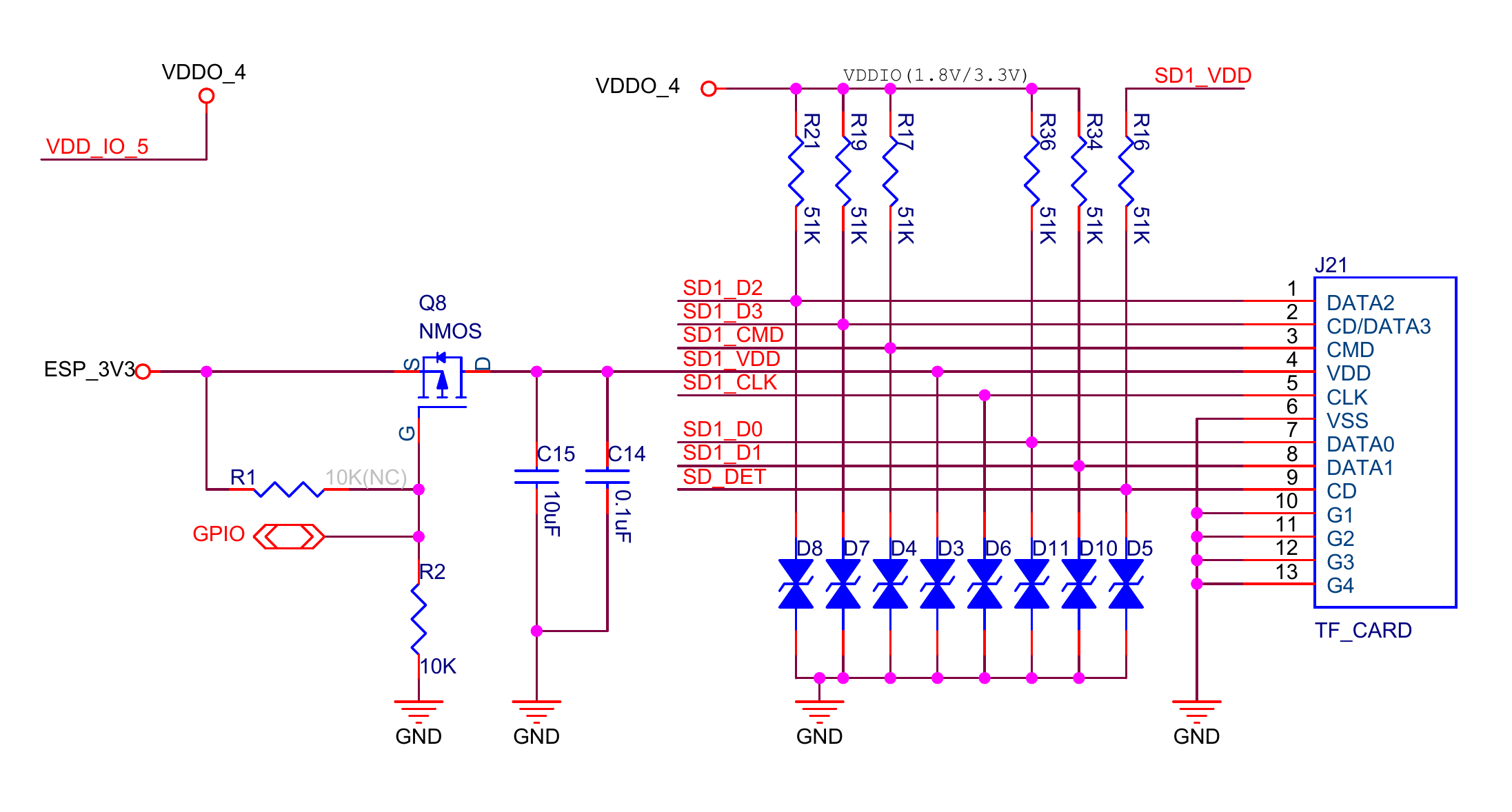
ESP32-P4 SD 3.0 Card Power Circuit
To reduce the power consumption of the SD card and reset it, you can populate a MOSFET at the power supply circuit of SD card and control it via GPIO.
USB
ESP32-P4 integrates a USB serial/JTAG controller that uses GPIO24 and GPIO25 as USB D- and USB D+ by default.
ESP32-P4 also features a USB 2.0 Full-Speed OTG peripheral with an integrated transceiver. By default, the USB 2.0 Full-Speed OTG uses GPIO26 and GPIO27 as USB D- and USB D+.
When using the USB serial/JTAG controller and USB 2.0 Full-Speed OTG, please note the following:
The roles of the USB D- and USB D+ pins can be swapped.
If only one function is in use, you can select either GPIO24/GPIO25 or GPIO26/GPIO27.
If both functions are used simultaneously, GPIO24/GPIO25 and GPIO26/GPIO27 will serve as two separate pins for each function.
ESP32-P4 also features a USB 2.0 High-Speed OTG peripheral with an integrated transceiver, where DM and DP respectively serve as the USB D- and USB D+.
When using chip revisions v1.0 and v1.3 (not recommended for new designs), add a 1 MΩ pull-down resistor on the DP pin to reduce the large transient current on VDD_USBPHY when CHIP_PU is pulled low.
DP Pull-down Resistor (Chip Revisions v1.0 and v1.3)
In chip revisions v3.0 and later versions, this issue has been fixed, allowing the retention of a 1 MΩ pull-down resistor for design compatibility.
It is recommended to add a 22/33 Ω series resistor and optional ground capacitors on the D- and D+ lines of the USB 2.0 Full-Speed OTG. These components should be placed close to the chip end.
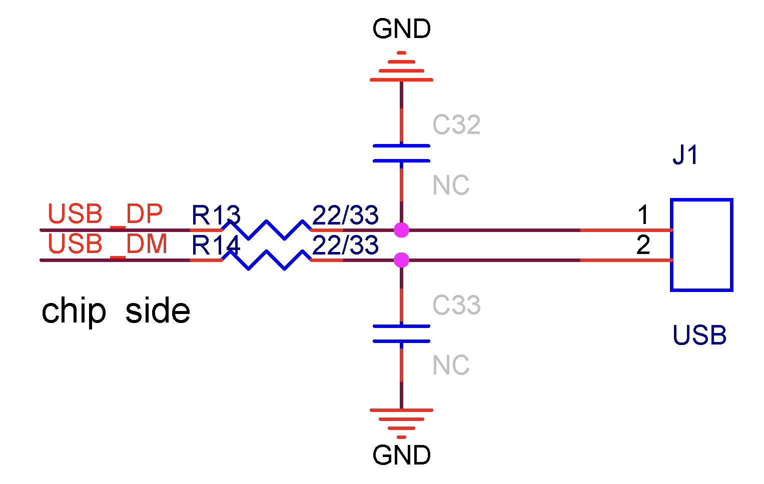
ESP32-P4 USB RC Circuit
At the USB connector end, it is advisable to include ESD protection diodes. When using the USB 2.0 High-Speed OTG peripheral, the parasitic capacitance of the diode should not exceed 1 pF to avoid poor signal quality and unstable transmission.
ESP32-P4 also supports downloading via USB. For details, please refer to Download Guidelines.
Touch Sensor
ESP32-P4 has 14 capacitive-sensing GPIOs, which detect variations induced by touching or approaching the GPIOs with a finger or other objects. The low-noise nature of the design and the high sensitivity of the circuit allow relatively small pads to be used. Arrays of pads can also be used, so that a larger area or more points can be detected.
The touch sensing performance can be further enhanced by the waterproof design, detection of frequency hopping, and digital filtering feature.
GPIO Pin Name |
Touch Sensor Function |
|---|---|
GPIO2 |
TOUCH_CHANNEL1 |
GPIO3 |
TOUCH_CHANNEL2 |
GPIO4 |
TOUCH_CHANNEL3 |
GPIO5 |
TOUCH_CHANNEL4 |
GPIO6 |
TOUCH_CHANNEL5 |
GPIO7 |
TOUCH_CHANNEL6 |
GPIO8 |
TOUCH_CHANNEL7 |
GPIO9 |
TOUCH_CHANNEL8 |
GPIO10 |
TOUCH_CHANNEL9 |
GPIO11 |
TOUCH_CHANNEL10 |
GPIO12 |
TOUCH_CHANNEL11 |
GPIO13 |
TOUCH_CHANNEL12 |
GPIO14 |
TOUCH_CHANNEL13 |
GPIO15 |
TOUCH_CHANNEL14 |
When using the touch function, it is recommended to populate a series resistor at ESP32-P4 side to reduce the coupling noise and interference on the line, and to strengthen the ESD protection. The recommended resistance is from 470 Ω to 2 kΩ, preferably 510 Ω. The specific value depends on the actual test results of the product.
Ethernet MAC
Refer to the table below for the GPIO configuration of the EMAC RMII interface.
Signal |
Pin Name |
|---|---|
RMII_CRSDV |
GPIO28, GPIO45, GPIO51 |
RMII_RXD0 |
GPIO29, GPIO46, GPIO52 |
RMII_RXD1 |
GPIO30, GPIO47, GPIO53 |
RMII_RXER |
GPIO31, GPIO48, GPIO54 |
RMII_CLK |
GPIO32, GPIO44, GPIO50 |
RMII_TXEN |
GPIO33, GPIO40, GPIO49 |
RMII_TXD0 |
GPIO34, GPIO41 |
RMII_TXD1 |
GPIO35, GPIO42 |
RMII_TXER |
GPIO36, GPIO43 |
It is recommended to populate a series resistor on the RMII CLK line.
Please note that the clock signal in the RMII interface is input-only. If you need a clock output solution, please use the REF_50M_CLK_PAD signal (GPIO23/GPIO39).
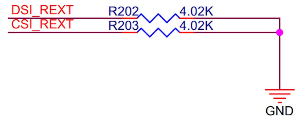
MIPI
ESP32-P4 includes an MIPI DSI interface for connecting displays with an MIPI interface, and an MIPI CSI interface for connecting cameras with an MIPI interface. Please populate a 4.02 kΩ pull-down resistor to both the CSI_REXT pin and DSI_REXT pin.
It is recommended to reserve series resistors on the MIPI communication lines (initially 0 Ω). The main purposes are to reduce drive current, adjust timing, and improve interference resistance.
If an RF module is included in the design, please also add series resistors on the CSI interface at the device end to minimize interference with the RF module.
Attention
If the MIPI interface is not used, the power and external resistor pins can be left floating.
For MIPI interface devices, please use GPIO for control signals.
ESP32-P4 Schematic for MIPI Signal