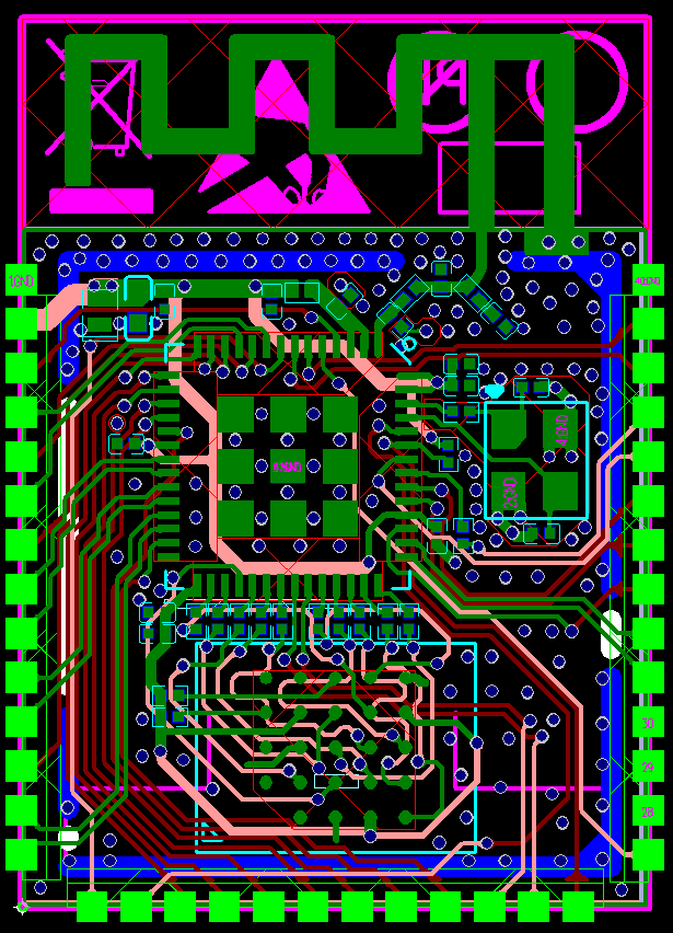
This chapter introduces the key points of how to design an ESP32-S3 PCB layout using an ESP32-S3 module (see Figure ESP32-S3 Reference PCB Layout) as an example.
Layer 2 (GND): No signal traces here to ensure a complete GND plane.
Layer 3 (POWER): GND plane should be applied to better isolate the RF and crystal. Route power traces and a few signal traces on this layer, provided that there is a complete GND plane under the RF and crystal.
Layer 4 (BOTTOM): Route a few signal traces here. It is not recommended to place any components on this layer.
A two-layer PCB design can also be used:
Layer 1 (TOP): Signal traces and components.
Layer 2 (BOTTOM): Do not place any components on this layer and keep traces to a minimum. Please make sure there is a complete GND plane for the chip, RF, and crystal.
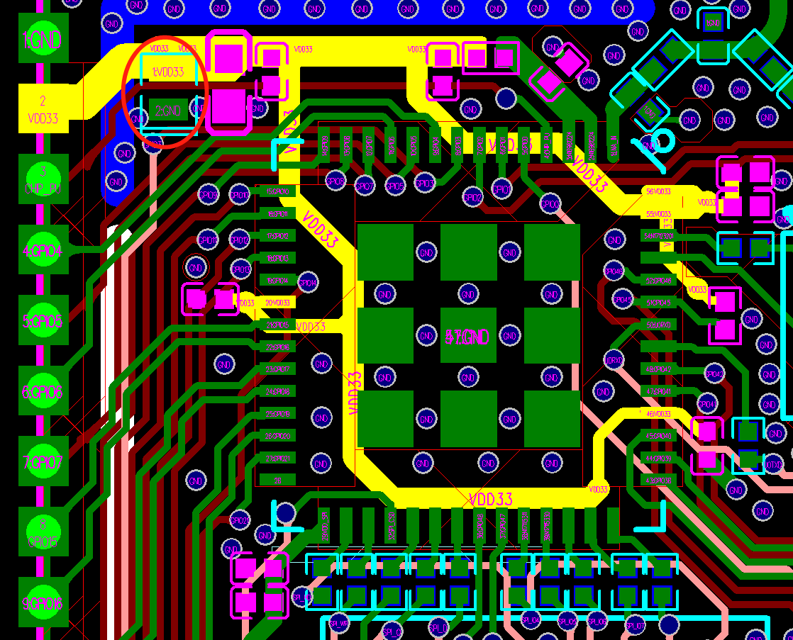
A four-layer PCB design is recommended. Whenever possible, route the power traces on the inner layers (not the ground layer) and connect them to the chip pins through vias. There should be at least two vias if the main power traces need to cross layers. The drill diameter on other power traces should be no smaller than the width of the power traces.
The yellow highlighted traces in Figure ESP32-S3 Power Traces in a Four-Layer PCB Design are the 3.3 V power traces. The width of the main power traces should be no less than 25 mil. The width of VDD3P3 at pin2 and pin3 power traces should be no less than 20 mil. The recommended width of other power traces is 10 mil. Ensure the power traces are surrounded by ground copper.
The red circles in ESP32-S3 Power Traces in a Four-Layer PCB Design show ESD protection diodes. Place them close to the power input. Add a 10 µF capacitor before the power trace enters the chip. You can also add a 0.1 µF or 1 µF capacitor in parallel. After that, the power trace can branch out in a star-shaped layout to reduce coupling between different power pins.
The power supply for pin2 and pin3 is RF related, so please place a 10 µF capacitor for each pin. You can also add a 0.1 µF or 1 µF capacitor in parallel.
Add a CLC/LC filter circuit near pin2 and pin3 to suppress high-frequency harmonics. The power trace can be routed at a 45-degree angle to maintain distance from adjacent RF traces. Except for the 10 µF capacitor, it is recommended to use 0201 components. This allows the filter circuit for pin2 and pin3 to be placed closer to the pins, with a GND isolation layer separating them from surrounding RF and GPIO traces, while also maximizing the placement of ground vias. Using 0201 components enables placing a via to the bottom layer at the first capacitor near the chip, while maintaining a keep-out area on other layers, further reducing harmonic interference. See Figure ESP32-S3 Power Traces in a Four-Layer PCB Design.
In Figure ESP32-S3 Power Traces in a Four-Layer PCB Design, the 10 µF capacitor is shared by the analog power supply VDD3P3 at pin2 and pin3, and the power entrance since the analog power is close to the chip power entrance. If the chip power entrance is not near VDD3P3 at pin2 and pin3, it is recommended to add a 10 µF capacitor to both the chip power entrance and VDD3P3 at pin2 and pin3.
Place appropriate decoupling capacitors at the rest of the power pins. Ground vias should be added close to the capacitor’s ground pad to ensure a short return path.
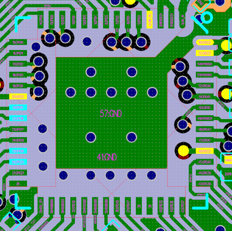
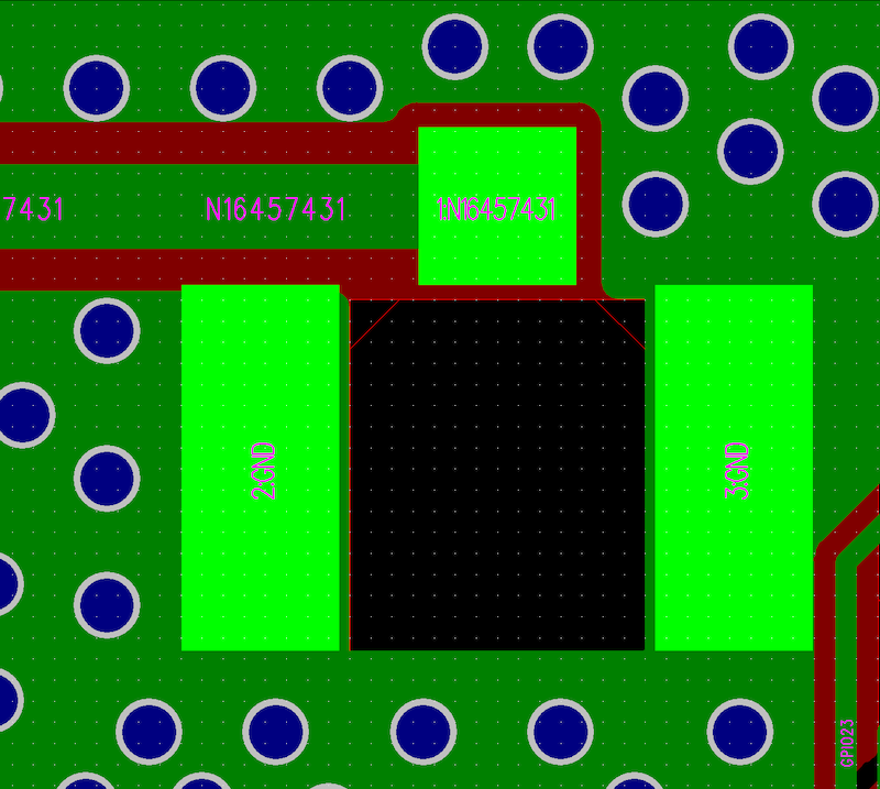
The ground pad at the bottom of the chip should be connected to the ground plane through at least nine ground vias.
The ground pads of the chip and surrounding circuit components should make full contact with the ground copper pour rather than being connected via traces.
If you need to add a thermal pad EPAD under the chip on the bottom of the module, it is recommended to employ a square grid on the EPAD, cover the gaps with solder paste, and place ground vias in the gaps, as shown in Figure ESP32-S3 Power Traces in a Four-Layer PCB Design. This helps effectively reduce solder leakage issues when soldering the module EPAD to the substrate.
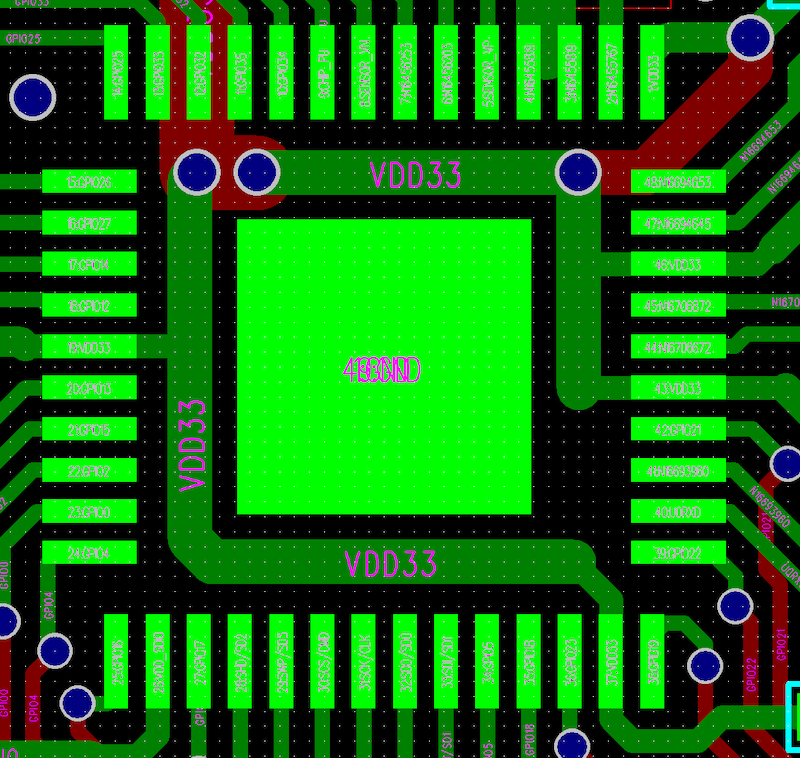
For optimal grounding, connect the EPAD to a large external ground area using wide traces or copper planes. See the figure below.
For a two-layer design, ensure to provide a continuous reference ground for the chip, RF, and crystal oscillator, as shown in the figure above.
In the figure above, the trace VDD33 represents the 3.3 V power trace. Unlike a four-layer design, the power trace should be routed on the top layer as much as possible. Therefore, the thermal pad in the center of the chip should be reduced in size, allowing the power trace to pass between the signal pads and the thermal pad. Vias to the bottom layer should only be used when absolutely necessary.
Other layout considerations are the same as for a four-layer design.
Note that there are no official two-layer modules. The figure above uses the ESP32 module as an example.
Figure ESP32-S3 Crystal Layout (with Keep-out Area on Top Layer) shows a reference PCB layout where the crystal is connected to the ground through vias and a keep-out area is maintained around the crystal on the top layer for ground isolation.
ESP32-S3 Crystal Layout (with Keep-out Area on Top Layer)
ESP32-S3 Crystal Layout (without Keep-out Area on Top Layer)
If there is sufficient ground on the top layer, it is recommended to maintain a keep-out area around the crystal for ground isolation. This helps to reduce the value of parasitic capacitance and suppress temperature conduction, which can otherwise affect the frequency offset. If there is no sufficient ground, do not maintain any keep-out area.
The layout of the crystal should follow the guidelines below:
Ensure a complete GND plane for the RF, crystal, and chip.
The crystal should be placed far from the clock pin to avoid interference on the chip. The gap should be at least 2.0 mm. It is good practice to add high-density ground vias stitching around the clock trace for better isolation.
There should be no vias for the clock input and output traces.
Components in series to the crystal trace should be placed close to the chip side.
The external matching capacitors should be placed on the two sides of the crystal, preferably at the end of the clock trace, but not connected directly to the series components. This is to make sure the ground pad of the capacitor is close to that of the crystal.
Do not route high-frequency digital signal traces under the crystal. It is best not to route any signal trace under the crystal. The vias on the power traces on both sides of the crystal clock trace should be placed as far away from the clock trace as possible, and the two sides of the clock trace should be surrounded by ground copper.
As the crystal is a sensitive component, do not place any magnetic components nearby that may cause interference, for example large inductance component, and ensure that there is a clean large-area ground plane around the crystal.
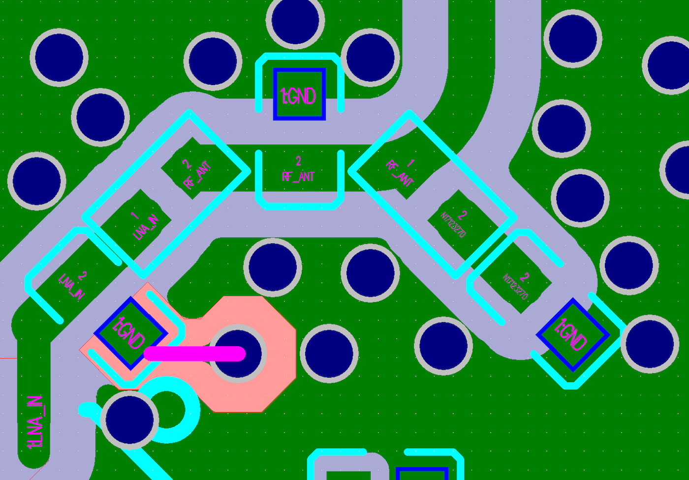
The RF layout should meet the following guidelines:
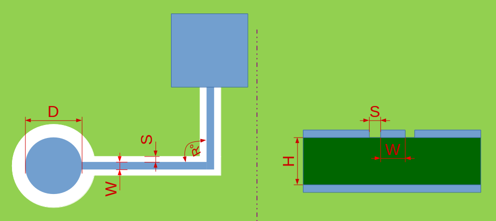
The RF trace should have a 50 Ω characteristic impedance. The reference plane is the layer next to the chip. For designing the RF trace at 50 Ω impedance, you could refer to the PCB stack-up design shown below.
A CLC matching circuit is required for chip tuning. Please use 0201 components and place them close to the pin in a zigzag. In other words, the two capacitors should not be oriented in the same direction to minimize interference.
Add a stub on the ground pad of the grounding capacitor near the chip side in the matching circuit to suppress the second harmonics. It is preferable to keep the stub length 15 mil, and determine the stub width according to the PCB stack-up so that the characteristic impedance of the stub is 100 Ω ± 10%. The reference plane is the third layer, so the area under the trace on the second layer should be cleared. The trace highlighted in Figure ESP32-S3 Stub in a Four-layer PCB Design is the stub. Note that a stub is not required for package types of 0402 and above.
For PCB antennas, make sure to validate them through both simulation and real-world testing on a development board. It is recommended to include an additional CLC matching circuit for antenna tuning. Place this circuit as close to the antenna as possible.
The RF trace should have a consistent width and not branch out. It should be as short as possible with dense ground vias around for interference shielding.
The RF trace should be routed on the outer layer without vias, i.e., should not cross layers. The RF trace should be routed at a 135° angle, or with circular arcs if trace bends are required.
The ground plane on the adjacent layer needs to be complete. Do not route any traces under the RF trace whenever possible.
There should be no high-frequency signal traces routed close to the RF trace. The RF antenna should be placed away from high-frequency components, such as crystals, DDR SDRAM, high-frequency clocks, etc. In addition, the USB port, USB-to-serial chip, UART signal lines (including traces, vias, test points, header pins, etc.) must be as far away from the antenna as possible. The UART signal line should be surrounded by ground copper and ground vias.
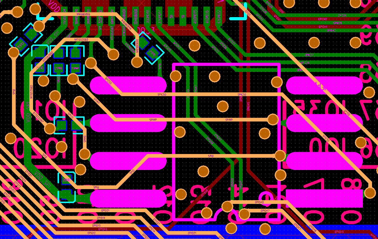
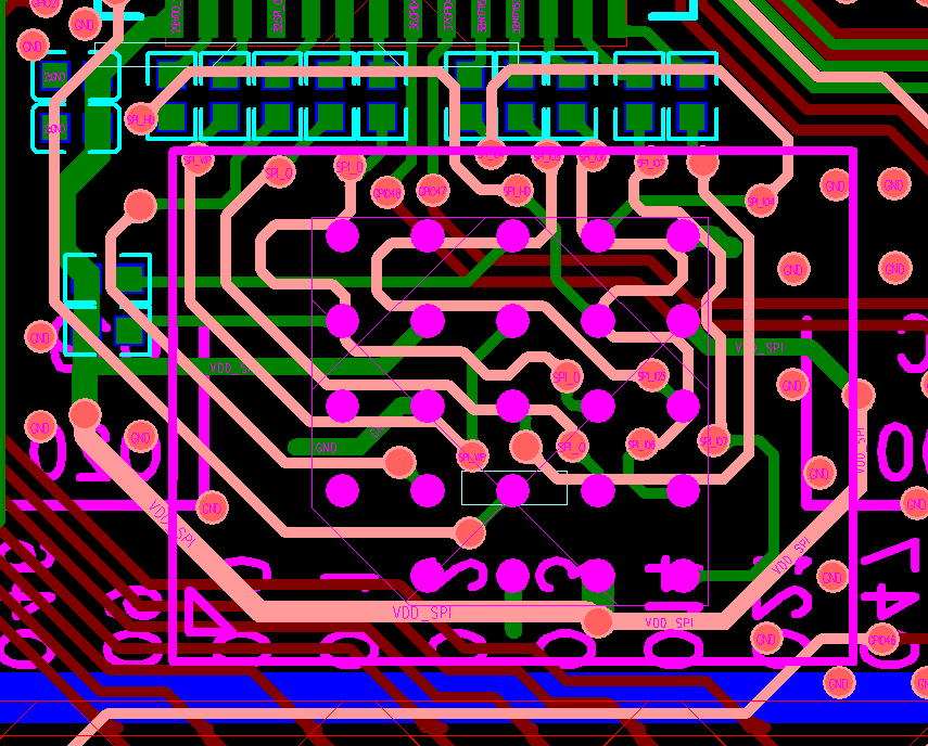
The layout for flash and PSRAM should follow the guidelines below:
Place the zero-ohm resistors in series on the SPI lines close to ESP32-S3.
Route the SPI traces on the inner layer (e.g., the third layer) whenever possible, and add ground copper and ground vias around the clock and data traces of SPI separately.
Octal SPI traces should have matching lengths.
If the flash and PSRAM are located far from ESP32-S3, it is recommended to place appropriate decoupling capacitors both at VDD_SPI and near the flash and PSRAM power supply.
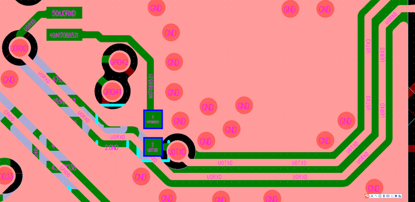
The UART layout should meet the following guidelines:
The series resistor on the U0TXD trace needs to be placed close to the chip side and away from the crystal.
The U0TXD and U0RXD traces on the top layer should be as short as possible.
The UART trace should be surrounded by ground copper and ground vias stitching.
General Principles of PCB Layout for Modules (Positioning a Module on a Base Board)
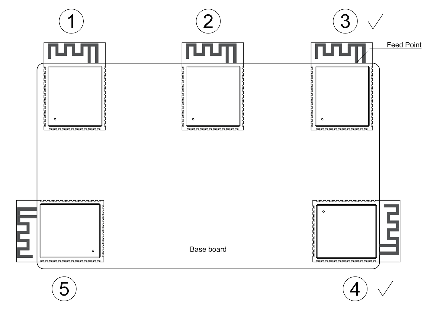
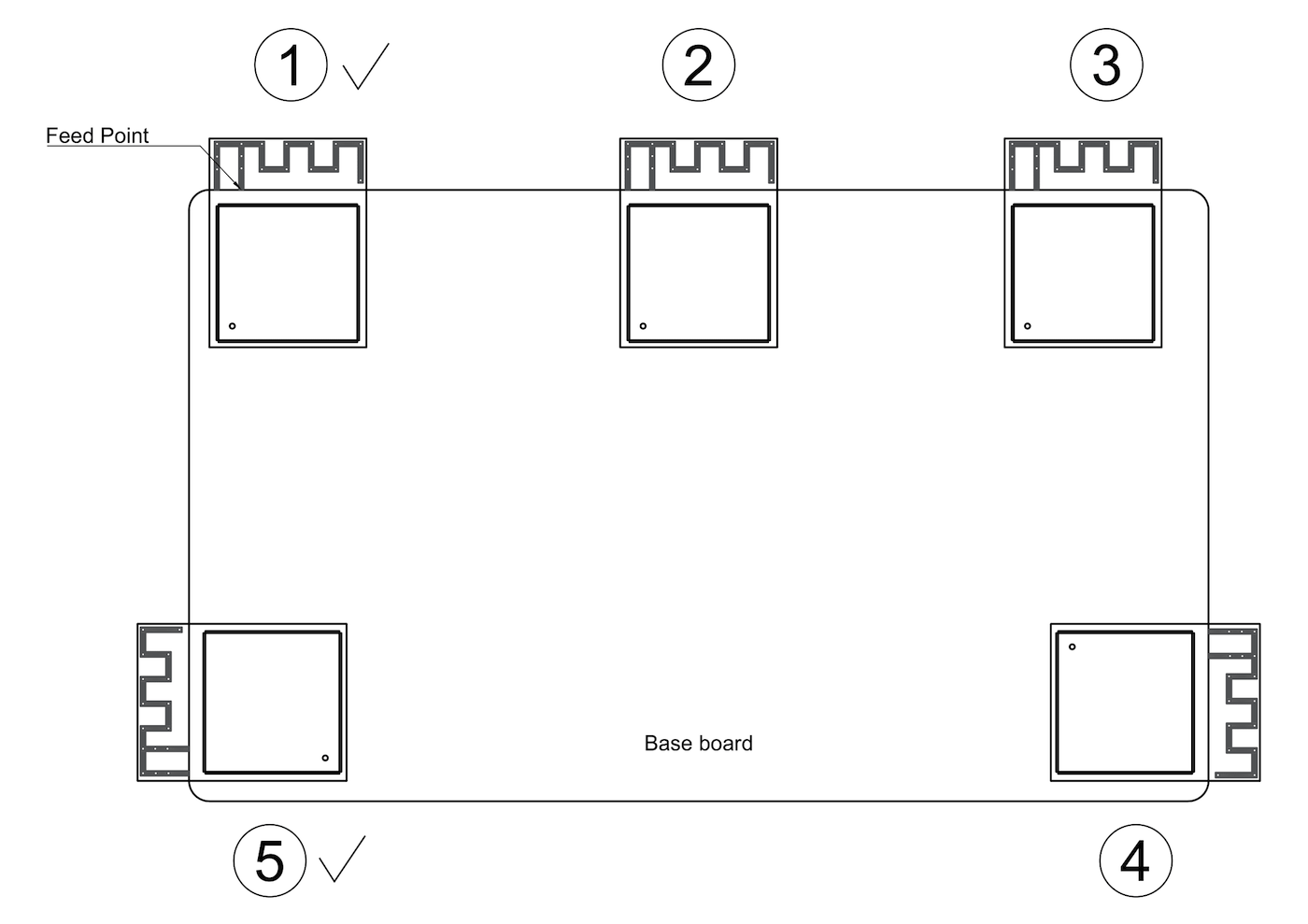
If module-on-board design is adopted, attention should be paid while positioning the module on the base board. The interference of the baseboard on the module’s antenna performance should be minimized.
It is suggested to place the module’s on-board PCB antenna outside the base board, and the feed point of the antenna close to the edge of the base board. In the following example figures, positions with mark ✓ are strongly recommended, while positions without a mark are not recommended.
Placement of ESP32-S3 Modules on Base Board (antenna feed point on the right)
Placement of ESP32-S3 Modules on Base Board (antenna feed point on the left)
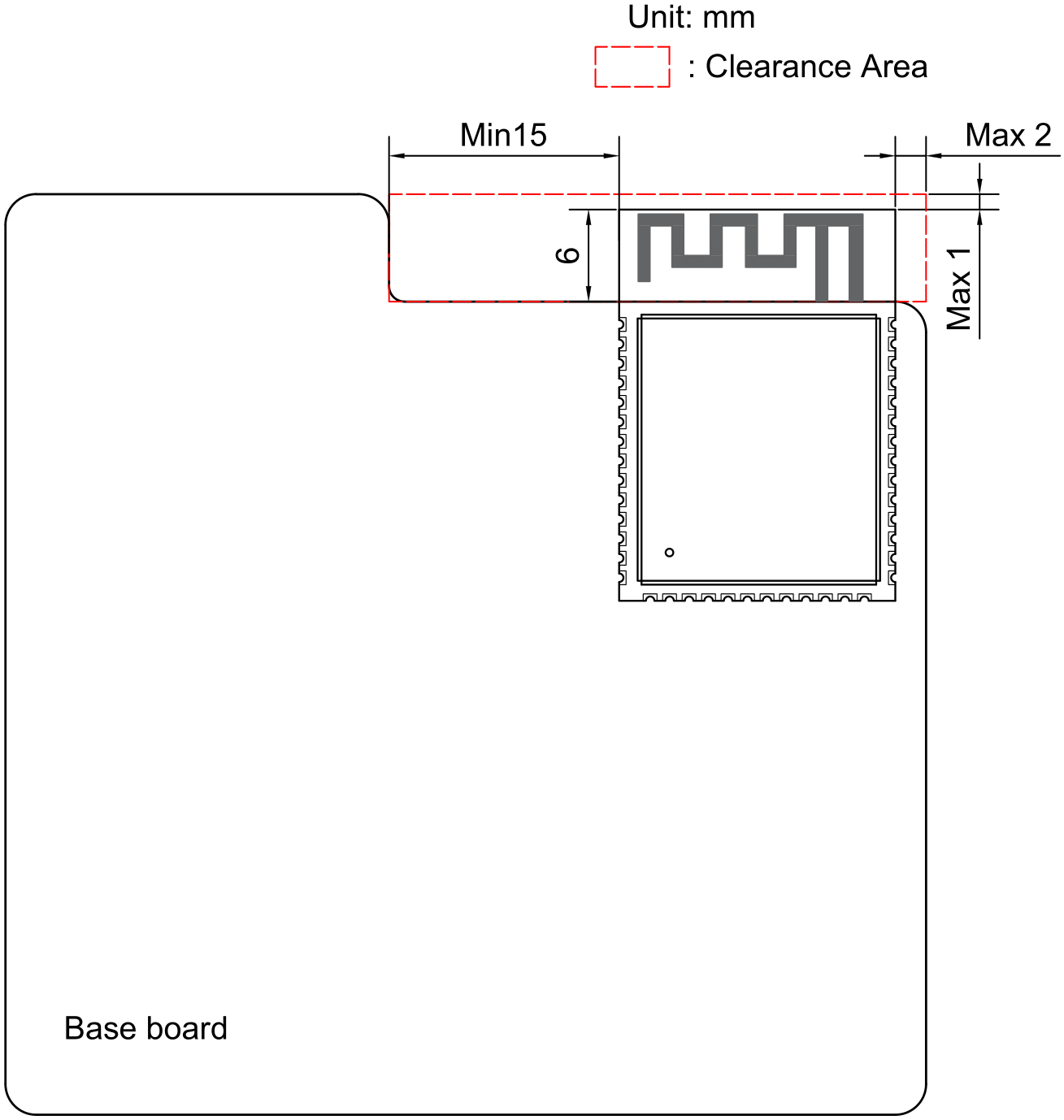
If the antenna cannot extend beyond the board edge, the feed point should still be placed as close to the board edge as possible. Then cut off the base board on both sides of the antenna and below it to minimize the impact of the base board material on the PCB antenna and provide a sufficiently large clearance area for the PCB antenna. Note that the module should not be placed in the center of the board with clearance created by hollowing out on all four sides. Figure Keepout Zone for ESP32-S3 Module’s Antenna (Antenna feed point on the Left) shows the suggested clearance area. Please note that sufficient ground copper and dense ground vias should be placed on the base board near the antenna.
Keepout Zone for ESP32-S3 Module’s Antenna (Antenna feed point on the Left)
After the base board is placed in the end product, please consider the impact of the housing on the antenna during end-product design. Ensure that the PCB antenna on the base board also has a sufficiently large clearance area inside the housing. A clearance of at least 15 mm is recommended in all directions.
Please note that the final end product should be tested for throughput and communication range to ensure RF performance.
The USB layout should meet the following guidelines:
Reserve space for resistors and capacitors on the USB traces close to the chip side.
Use differential pairs and route them in parallel at equal lengths. Maintain a differential pair impedance of 90 Ω with a tolerance of ±10%.
USB differential traces should minimize via transitions as much as possible to ensure better impedance control and avoid signal reflections. If vias are necessary, add a pair of ground return vias at each transition point.
Ensure there is a continuous reference layer (a ground layer is recommended) beneath the USB traces.
The SDIO layout should follow the guidelines below:
Minimize parasitic capacitance of SDIO traces as they involve high-speed signals.
The trace lengths for SDIO_CMD and SDIO_DATA0 ~ SDIO_DATA3 should be within ± 50 mil of the SDIO_CLK trace length. Use serpentine routing if necessary.
For SDIO routing, maintain a 50 Ω single-ended impedance with a tolerance of ±10%.
Keep the total trace length from SDIO GPIOs to the master SDIO interface as short as possible, ideally within 2000 mil.
Ensure that SDIO traces do not cross layers. Besides, a reference plane (preferably a ground plane) must be placed beneath the traces, and continuity of the reference plane must be ensured.
It is recommended to surround the SDIO_CLK trace with ground copper.
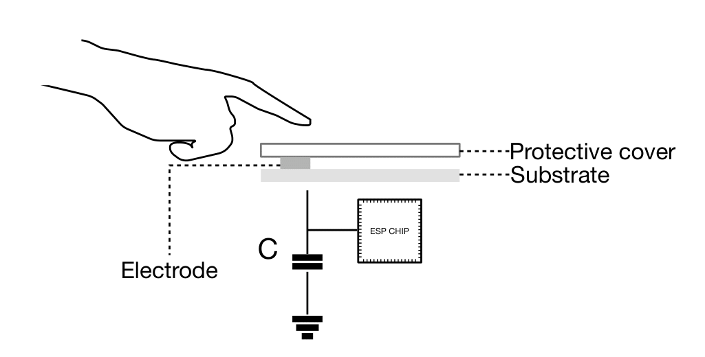
ESP32-S3 offers up to 14 capacitive IOs that detect changes in capacitance on touch sensors due to finger contact or proximity. The chip’s internal capacitance detection circuit features low noise and high sensitivity. It allows to use touch pads with smaller area to implement the touch detection function. You can also use the touch panel array to detect a larger area or more test points.
To prevent capacitive coupling and other electrical interference to the sensitivity of the touch sensor system, the following factors should be taken into account.
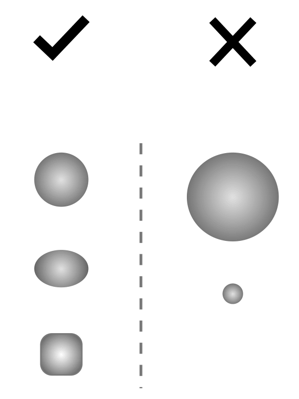
The proper size and shape of an electrode improves system sensitivity. Round, oval, or shapes similar to a human fingertip are commonly applied. Large size or irregular shape might lead to incorrect responses from nearby electrodes.
Figure ESP32-S3 Electrode Pattern Requirements shows the proper and improper size or shape of electrode. Please note that the examples illustrated in the figure are not of actual scale. It is suggested to use a human fingertip as reference.
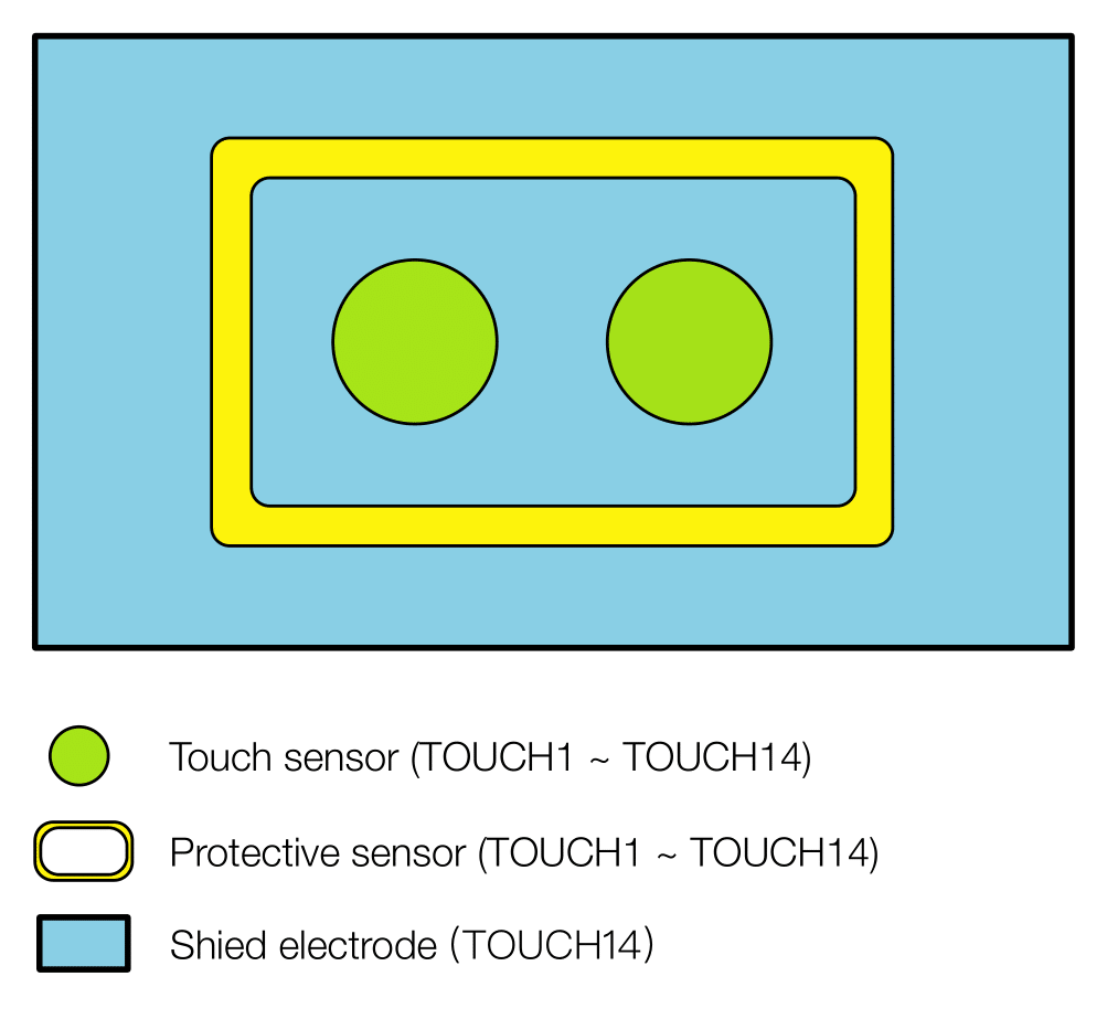
ESP32-S3 touch sensor has a waterproof design and features proximity sensor function. Figure ESP32-S3 Waterproof and Proximity Sensing Design shows an example layout of a waterproof and proximity sensing design.
Note the following guidelines to better implement the waterproof and proximity sensing design:
The recommended width of the shield electrode width is 2 cm.
Employ a grid on the top layer with a trace width of 7 mil and a grid width of 45 mil (25% fill). The filled grid is connected to the driver shield signal.
Employ a grid on the bottom layer with a trace width of 7 mil and a grid width of 70 mil (17% fill). The filled grid is connected to the driver shield signal.
The protective sensor should be in a rectangle shape with curved edges and surround all other sensors.
The recommended width of the protective sensor is 2 mm.
The recommended gap between the protective sensor and shield sensor is 1 mm.
The sensing distance of the proximity sensor is directly proportional to the area of the proximity sensor. However, increasing the sensing area will introduce more noise. Actual testing is needed for optimized performance.
It is recommended that the shape of the proximity sensor is a closed loop. The recommended width is 1.5 mm.
When ESP32-S3 sends data packages, the voltage ripple is small, but RF TX performance is poor.
Analysis: The RF TX performance can be affected not only by voltage ripples, but also by the crystal itself. Poor quality and big frequency offsets of the crystal decrease the RF TX performance. The crystal clock may be corrupted by other interfering signals, such as high-speed output or input signals. In addition, high-frequency signal traces, such as the SDIO traces and UART traces under the crystal, could also result in the malfunction of the crystal. Besides, sensitive components or radiating components, such as inductors and antennas, may also decrease the RF performance.
Solution: This problem is caused by improper layout for the crystal and can be solved by re-layout. Please refer to Section Crystal for details.
When ESP32-S3 sends data packages, the power value is much higher or lower than the target power value, and the EVM is relatively poor.
Analysis: The disparity between the tested value and the target value may be due to signal reflection caused by the impedance mismatch on the transmission line connecting the RF pin and the antenna. Besides, the impedance mismatch will affect the working state of the internal PA, making the PA prematurely access the saturated region in an abnormal way. The EVM becomes poor as the signal distortion happens.
Solution: Match the antenna’s impedance with the π-type circuit on the RF trace, so that the impedance of the antenna as seen from the RF pin matches closely with that of the chip. This reduces reflections to the minimum.
TX performance is not bad, but the RX sensitivity is low.
Analysis: Good TX performance indicates proper RF impedance matching. Poor RX sensitivity may result from external coupling to the antenna. For instance, the crystal signal harmonics could couple to the antenna. If the TX and RX traces of UART cross over with RF trace, they will affect the RX performance, as well. If there are many high-frequency interference sources on the board, signal integrity should be considered.
Solution: Keep the antenna away from crystals. Do not route high-frequency signal traces close to the RF trace. Please refer to Section RF for details.