ESP-WROVER-KIT V3 Getting Started Guide (CMake)
This user guide shows how to get started with ESP-WROVER-KIT V3 development board including description of its functionality and configuration options. For description of other versions of the ESP-WROVER-KIT check ESP32 Hardware Reference.
What You Need
1 x Micro USB 2.0 Cable, Type A to Micro B
1 × PC loaded with Windows, Linux or Mac OS
If you want to start using this board right now, go directly to Section Start Application Development.
Overview
The ESP-WROVER-KIT is a development board produced by Espressif built around ESP32. This board is compatible with ESP32 modules, including the ESP-WROOM-32 and ESP32-WROVER. The ESP-WROVER-KIT features support for an LCD and MicroSD card. The I/O pins have been broken out from the ESP32 module for easy extension. The board carries an advanced multi-protocol USB bridge (the FTDI FT2232HL), enabling developers to use JTAG directly to debug the ESP32 through the USB interface. The development board makes secondary development easy and cost-effective.
Note
ESP-WROVER-KIT V3 integrates the ESP32-WROVER module by default.
Functionality Overview
Block diagram below presents main components of ESP-WROVER-KIT and interconnections between components.
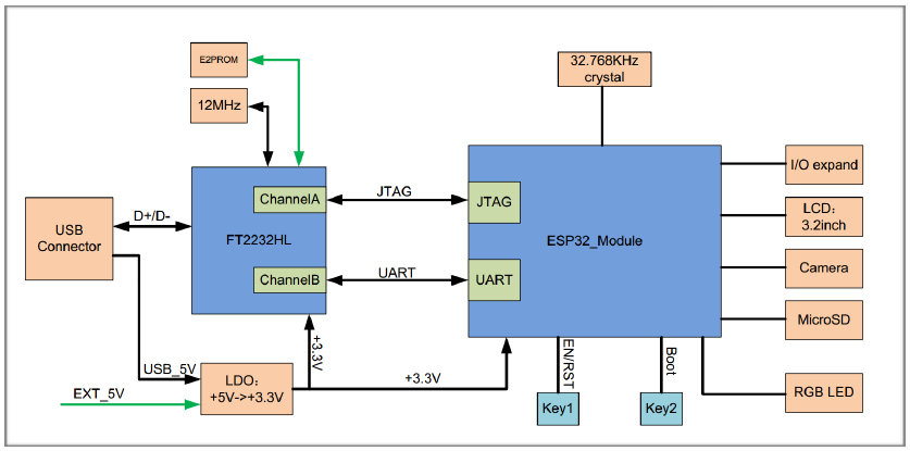
ESP-WROVER-KIT block diagram
Functional Description
The following list and figures below describe key components, interfaces and controls of ESP-WROVER-KIT board.
- 32.768 kHz
An external precision 32.768 kHz crystal oscillator provides the chip with a clock of low-power consumption during the Deep-sleep mode.
- 0R
A zero Ohm resistor intended as a placeholder for a current shunt. May be desoldered or replaced with a current shunt to facilitate measurement of current required by ESP32 module depending on power mode.
- ESP32 Module
ESP-WROVER-KIT is compatible with both ESP-WROOM-32 and ESP32-WROVER. The ESP32-WROVER module features all the functions of ESP-WROOM-32 and integrates an external 32-MBit PSRAM for flexible extended storage and data processing capabilities.
Note
GPIO16 and GPIO17 are used as the CS and clock signal for PSRAM. To ensure reliable performance, the two GPIOs are not broken out.
- FT2232
The FT2232 chip is a multi-protocol USB-to-serial bridge. Users can control and program the FT2232 chip through the USB interface to establish communication with ESP32. The FT2232 chip also features USB-to-JTAG interface. USB-to-JTAG is available on channel A of FT2232, USB-to-serial on channel B. The embedded FT2232 chip is one of the distinguishing features of the ESPWROVER-KIT. It enhances users’ convenience in terms of application development and debugging. In addition, users do not need to buy a JTAG debugger separately, which reduces the development cost, see ESP-WROVER-KIT V3 schematic.
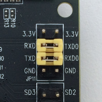
- UART
Serial port: the serial TX/RX signals on FT2232HL and ESP32 are broken out to the two sides of JP11. By default, the two signals are connected with jumpers. To use the ESP32 module serial interface only, the jumpers may be removed and the module can be connected to another external serial device.
- SPI
SPI interface: the SPI interface connects to an external flash (PSRAM). To interface another SPI device, an extra CS signal is needed. The electrical level on the flash of this module is 1.8V. If an ESP-WROOM-32 is being used, please note that the electrical level on the flash of this module is 3.3V.
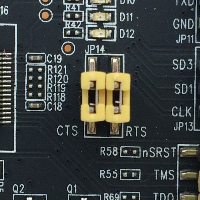
- CTS/RTS
Serial port flow control signals: the pins are not connected to the circuitry by default. To enable them, respective pins of JP14 must be shorted with jumpers.
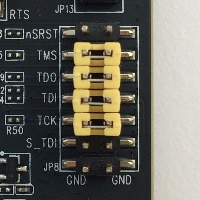
- JTAG
JTAG interface: the JTAG signals on FT2232HL and ESP32 are broken out to the two sides of JP8. By default, the two signals are disconnected. To enable JTAG, shorting jumpers are required on the signals.
- EN
Reset button: pressing this button resets the system.
- Boot
Download button: holding down the Boot button and pressing the EN button initiates the firmware download mode. Then user can download firmware through the serial port.
- USB
USB interface. It functions as the power supply for the board and the communication interface between PC and ESP32 module.
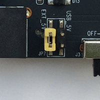
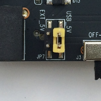
- Power Select
Power supply selection interface: the ESP-WROVER-KIT can be powered through the USB interface or the 5V Input interface. The user can select the power supply with a jumper. More details can be found in Section Setup Options, jumper header JP7.
- Power Key
Power on/off button: toggling to the right powers the board on; toggling to the left powers the board off.
- 5V Input
The 5V power supply interface is used as a backup power supply in case of full-load operation.
- LDO
NCP1117(1A). 5V-to-3.3V LDO. (There is an alternative pin-compatible LDO — LM317DCY, with an output current of up to 1.5A). NCP1117 can provide a maximum current of 1A. The LDO solutions are available with both fixed output voltage and variable output voltage. For details please refer to ESP-WROVER-KIT V3 schematic.
- Camera
Camera interface: a standard OV7670 camera module is supported.
- RGB
Red, green and blue (RGB) light emitting diodes (LEDs), which may be controlled by pulse width modulation (PWM).
- I/O
All the pins on the ESP32 module are led out to the pin headers on the ESP-WROVER-KIT. Users can program ESP32 to enable multiple functions such as PWM, ADC, DAC, I2C, I2S, SPI, etc.
- Micro SD Card
Micro SD card slot for data storage.
- LCD
ESP-WROVER-KIT supports mounting and interfacing a 3.2” SPI (standard 4-wire Serial Peripheral Interface) LCD, as shown on figure ESP-WROVER-KIT board layout - back.
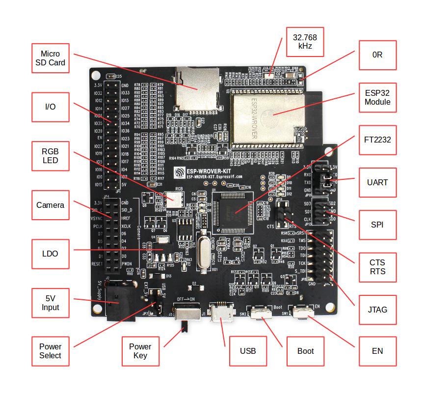
ESP-WROVER-KIT board layout - front
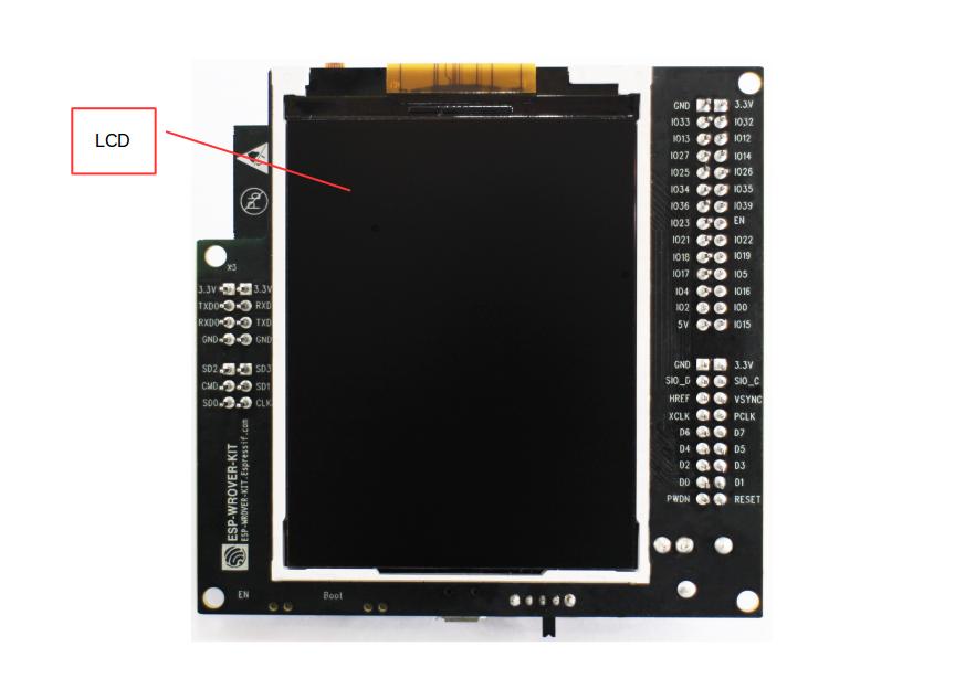
ESP-WROVER-KIT board layout - back
Setup Options
There are five jumper headers available to set up the board functionality. Typical options to select from are listed in table below.
Header |
Jumper Setting |
Description of Functionality |
JP7 |
|
Power ESP-WROVER-KIT board from an external power supply |
JP7 |
|
Power ESP-WROVER-KIT board from an USB port |
JP8 |
|
Enable JTAG functionality |
JP11 |
|
Enable UART communication |
JP14 |
|
Enable RTS/CTS flow control for serial communication |
Allocation of ESP32 Pins
Several pins / terminals of ESP32 module are allocated to the on board hardware. Some of them, like GPIO0 or GPIO2, have multiple functions. If certain hardware is not installed, e.g. nothing is plugged in to the Camera / JP4 header, then selected GPIOs may be used for other purposes.
Main I/O Connector / JP1
The JP1 connector is shown in two columns in the middle under “I/O” headers. The two columns “Shared With” outside, describe where else on the board certain GPIO is used.
Shared With |
I/O |
I/O |
Shared With |
|---|---|---|---|
3.3V |
GND |
||
NC/XTAL |
IO32 |
IO33 |
NC/XTAL |
JTAG, MicroSD |
IO12 |
IO13 |
JTAG, MicroSD |
JTAG, MicroSD |
IO14 |
IO27 |
Camera |
Camera |
IO26 |
IO25 |
Camera, LCD |
Camera |
IO35 |
IO34 |
Camera |
Camera |
IO39 |
IO36 |
Camera |
JTAG |
EN |
IO23 |
Camera, LCD |
Camera, LCD |
IO22 |
IO21 |
Camera, LCD, MicroSD |
Camera, LCD |
IO19 |
IO18 |
Camera, LCD |
Camera, LCD |
IO5 |
IO17 |
PSRAM |
PSRAM |
IO16 |
IO4 |
LED, Camera, MicroSD |
LED, Boot |
IO0 |
IO2 |
LED, Camera, MicroSD |
JTAG, MicroSD |
IO15 |
5V |
Legend:
NC/XTAL - 32.768 kHz Oscillator
JTAG - JTAG / JP8
Boot - Boot button / SW2
Camera - Camera / JP4
LED - RGB LED
MicroSD - MicroSD Card / J4
LCD - LCD / U5
PSRAM - ESP32-WROVER’s PSRAM, if ESP32-WROVER is installed
32.768 kHz Oscillator
ESP32 Pin |
|
|---|---|
1 |
GPIO32 |
2 |
GPIO33 |
Note
As GPIO32 and GPIO33 are connected to the oscillator, to maintain signal integrity, they are not connected to JP1 I/O expansion connector. This allocation may be changed from oscillator to JP1 by desoldering 0R resistors from positions R11 / R23 and installing them in positions R12 / R24.
SPI Flash / JP13
ESP32 Pin |
|
|---|---|
1 |
CLK / GPIO6 |
2 |
SD0 / GPIO7 |
3 |
SD1 / GPIO8 |
4 |
SD2 / GPIO9 |
5 |
SD3 / GPIO10 |
6 |
CMD / GPIO11 |
Important
The module’s flash bus is connected to the pin header JP13 through 0-Ohm resistors R140 ~ R145. If the flash frequency needs to operate at 80 MHz, to improve integrity of the bus signals, it is recommended to desolder resistors R140 ~ R145. At this point, the module’s flash bus is disconnected with the pin header JP13.
JTAG / JP8
ESP32 Pin |
JTAG Signal |
|
|---|---|---|
1 |
EN |
TRST_N |
2 |
MTDO / GPIO15 |
TDO |
3 |
MTDI / GPIO12 |
TDI |
4 |
MTCK / GPIO13 |
TCK |
5 |
MTMS / GPIO14 |
TMS |
Camera / JP4
ESP32 Pin |
Camera Signal |
|
|---|---|---|
1 |
GPIO27 |
SCCB Clock |
2 |
GPIO26 |
SCCB Data |
3 |
GPIO21 |
System Clock |
4 |
GPIO25 |
Vertical Sync |
5 |
GPIO23 |
Horizontal Reference |
6 |
GPIO22 |
Pixel Clock |
7 |
GPIO4 |
Pixel Data Bit 0 |
8 |
GPIO5 |
Pixel Data Bit 1 |
9 |
GPIO18 |
Pixel Data Bit 2 |
10 |
GPIO19 |
Pixel Data Bit 3 |
11 |
GPIO36 |
Pixel Data Bit 4 |
11 |
GPIO39 |
Pixel Data Bit 5 |
11 |
GPIO34 |
Pixel Data Bit 6 |
11 |
GPIO35 |
Pixel Data Bit 7 |
11 |
GPIO2 |
Camera Reset |
RGB LED
ESP32 Pin |
RGB LED |
|
|---|---|---|
1 |
GPIO0 |
Red |
2 |
GPIO2 |
Blue |
3 |
GPIO4 |
Green |
MicroSD Card / J4
ESP32 Pin |
MicroSD Signal |
|
|---|---|---|
1 |
MTDI / GPIO12 |
DATA2 |
2 |
MTCK / GPIO13 |
CD / DATA3 |
3 |
MTDO / GPIO15 |
CMD |
4 |
MTMS / GPIO14 |
CLK |
5 |
GPIO2 |
DATA0 |
6 |
GPIO4 |
DATA1 |
7 |
GPIO21 |
CD |
LCD / U5
ESP32 Pin |
LCD Signal |
|
|---|---|---|
1 |
GPIO18 |
RESET |
2 |
GPIO19 |
SCL |
3 |
GPIO21 |
D/C |
4 |
GPIO22 |
CS |
5 |
GPIO23 |
SDA |
6 |
GPIO25 |
SDO |
7 |
GPIO5 |
Backlight |
Start Application Development
Before powering up the ESP-WROVER-KIT, please make sure that the board has been received in good condition with no obvious signs of damage.
Initial Setup
Select the source of power supply for the board by setting jumper JP7. The options are either USB port or an external power supply. For this application selection of USB port is sufficient. Enable UART communication by installing jumpers on JP11. Both selections are shown in table below.
Power up from USB port |
Enable UART communication |
|
|
Do not install any other jumpers.
Now to Development
To start development of applications, proceed to Section Get Started (CMake), that will walk you through the Installation Step by Step.