Analog to Digital Converter
Overview
The ESP32 integrates two 12-bit SAR (Successive Approximation Register) ADCs supporting a total of 18 measurement channels (analog enabled pins).
The ADC driver API supports ADC1 (8 channels, attached to GPIOs 32 - 39), and ADC2 (10 channels, attached to GPIOs 0, 2, 4, 12 - 15 and 25 - 27). However, the usage of ADC2 has some restrictions for the application:
ADC2 is used by the Wi-Fi driver. Therefore the application can only use ADC2 when the Wi-Fi driver has not started.
Some of the ADC2 pins are used as strapping pins (GPIO 0, 2, 15) thus cannot be used freely. Such is the case in the following official Development Kits:
ESP32 DevKitC: GPIO 0 cannot be used due to external auto program circuits.
ESP-WROVER-KIT: GPIO 0, 2, 4 and 15 cannot be used due to external connections for different purposes.
Configuration and Reading ADC
The ADC should be configured before reading is taken.
For ADC1, configure desired precision and attenuation by calling functions
adc1_config_width()andadc1_config_channel_atten().For ADC2, configure the attenuation by
adc2_config_channel_atten(). The reading width of ADC2 is configured every time you take the reading.
Attenuation configuration is done per channel, see adc1_channel_t and adc2_channel_t, set as a parameter of above functions.
Then it is possible to read ADC conversion result with adc1_get_raw() and adc2_get_raw(). Reading width of ADC2 should be set as a parameter of adc2_get_raw() instead of in the configuration functions.
Note
Since the ADC2 is shared with the WIFI module, which has higher priority, reading operation of adc2_get_raw() will fail between esp_wifi_start() and esp_wifi_stop(). Use the return code to see whether the reading is successful.
It is also possible to read the internal hall effect sensor via ADC1 by calling dedicated function hall_sensor_read(). Note that even the hall sensor is internal to ESP32, reading from it uses channels 0 and 3 of ADC1 (GPIO 36 and 39). Do not connect anything else to these pins and do not change their configuration. Otherwise it may affect the measurement of low value signal from the sensor.
This API provides convenient way to configure ADC1 for reading from ULP. To do so, call function adc1_ulp_enable() and then set precision and attenuation as discussed above.
There is another specific function adc2_vref_to_gpio() used to route internal reference voltage to a GPIO pin. It comes handy to calibrate ADC reading and this is discussed in section Minimizing Noise.
Application Examples
Reading voltage on ADC1 channel 0 (GPIO 36):
#include <driver/adc.h>

...

    adc1_config_width(ADC_WIDTH_BIT_12);
    adc1_config_channel_atten(ADC1_CHANNEL_0,ADC_ATTEN_DB_0);
    int val = adc1_get_raw(ADC1_CHANNEL_0);
The input voltage in above example is from 0 to 1.1V (0 dB attenuation). The input range can be extended by setting higher attenuation, see adc_atten_t.
An example using the ADC driver including calibration (discussed below) is available in esp-idf: peripherals/adc
Reading voltage on ADC2 channel 7 (GPIO 27):
#include <driver/adc.h>

...

    int read_raw;
    adc2_config_channel_atten( ADC2_CHANNEL_7, ADC_ATTEN_0db );

    esp_err_t r = adc2_get_raw( ADC2_CHANNEL_7, ADC_WIDTH_12Bit, &read_raw);
    if ( r == ESP_OK ) {
        printf("%d\n", read_raw );
    } else if ( r == ESP_ERR_TIMEOUT ) {
        printf("ADC2 used by Wi-Fi.\n");
    }
The reading may fail due to collision with Wi-Fi, should check it. An example using the ADC2 driver to read the output of DAC is available in esp-idf: peripherals/adc2
Reading the internal hall effect sensor:
#include <driver/adc.h>

...

    adc1_config_width(ADC_WIDTH_BIT_12);
    int val = hall_sensor_read();
The value read in both these examples is 12 bits wide (range 0-4095).
Minimizing Noise
The ESP32 ADC can be sensitive to noise leading to large discrepancies in ADC readings. To minimize noise, users may connect a 0.1uF capacitor to the ADC input pad in use. Multisampling may also be used to further mitigate the effects of noise.
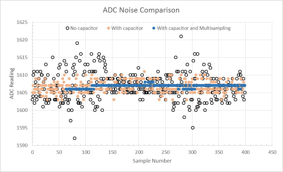
Graph illustrating noise mitigation using capacitor and multisampling of 64 samples.
ADC Calibration
The esp_adc_cal/include/esp_adc_cal.h API provides functions to correct for differences in measured voltages caused by variation of ADC reference voltages (Vref) between chips. Per design the ADC reference voltage is 1100mV, however the true reference voltage can range from 1000mV to 1200mV amongst different ESP32s.
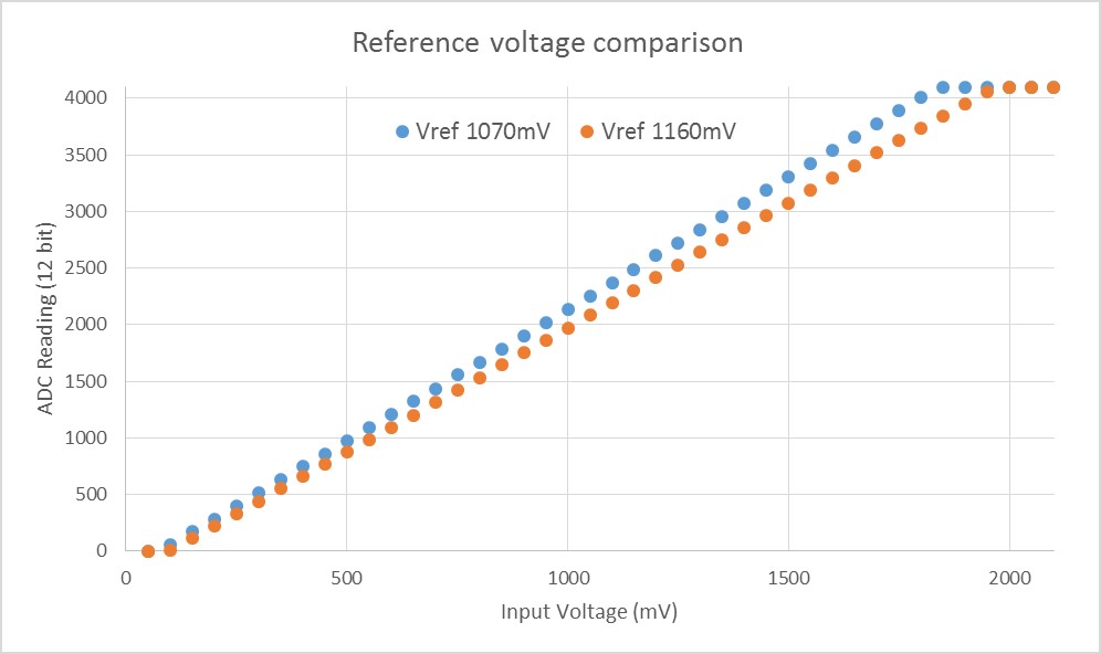
Graph illustrating effect of differing reference voltages on the ADC voltage curve.
Correcting ADC readings using this API involves characterizing one of the ADCs at a given attenuation to obtain a characteristics curve (ADC-Voltage curve) that takes into account the difference in ADC reference voltage. The characteristics curve is in the form of y = coeff_a * x + coeff_b and is used to convert ADC readings to voltages in mV. Calculation of the characteristics curve is based on calibration values which can be stored in eFuse or provided by the user.
Calibration Values
Calibration values are used to generate characteristic curves that account for the unique ADC reference voltage of a particular ESP32. There are currently three sources of calibration values. The availability of these calibration values will depend on the type and production date of the ESP32 chip/module.
Two Point values represent each of the ADCs’ readings at 150mV and 850mV. To obtain more accurate calibration results these values should be measured by user and burned into eFuse
BLOCK3.eFuse Vref represents the true ADC reference voltage. This value is measured and burned into eFuse
BLOCK0during factory calibration.Default Vref is an estimate of the ADC reference voltage provided by the user as a parameter during characterization. If Two Point or eFuse Vref values are unavailable, Default Vref will be used.
Individual measurement and burning of the eFuse Vref has been applied to ESP32-D0WD and ESP32-D0WDQ6 chips produced on/after the 1st week of 2018. Such chips may be recognized by date codes on/later than 012018 (see Line 4 on figure below).
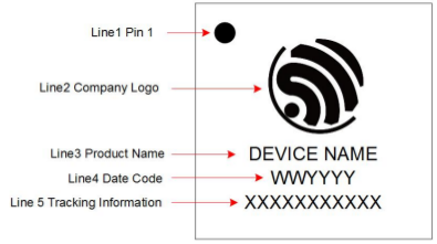
ESP32 Chip Surface Marking
If you would like to purchase chips or modules with calibration, double check with distributor or Espressif directly.
If you are unable to check the date code (i.e. the chip may be enclosed inside a canned module, etc.), you can still verify if eFuse Vref is present by running espefuse.py tool with adc_info parameter
$IDF_PATH/components/esptool_py/esptool/espefuse.py --port /dev/ttyUSB0 adc_info
Replace /dev/ttyUSB0 with ESP32 board’s port name.
A chip that has specific eFuse Vref value programmed (in this case 1093mV) will be reported as follows:
ADC VRef calibration: 1093mV
In another example below the eFuse Vref is not programmed:
ADC VRef calibration: None (1100mV nominal)
For a chip with two point calibration the message will look similar to:
ADC VRef calibration: 1149mV
ADC readings stored in efuse BLK3:
    ADC1 Low reading  (150mV): 306
    ADC1 High reading (850mV): 3153
    ADC2 Low reading  (150mV): 389
    ADC2 High reading (850mV): 3206
Application Example
For a full example see esp-idf: peripherals/adc
Characterizing an ADC at a particular attenuation:
#include "driver/adc.h"
#include "esp_adc_cal.h"

...

    //Characterize ADC at particular atten
    esp_adc_cal_characteristics_t *adc_chars = calloc(1, sizeof(esp_adc_cal_characteristics_t));
    esp_adc_cal_value_t val_type = esp_adc_cal_characterize(unit, atten, ADC_WIDTH_BIT_12, DEFAULT_VREF, adc_chars);
    //Check type of calibration value used to characterize ADC
    if (val_type == ESP_ADC_CAL_VAL_EFUSE_VREF) {
        printf("eFuse Vref");
    } else if (val_type == ESP_ADC_CAL_VAL_EFUSE_TP) {
        printf("Two Point");
    } else {
        printf("Default");
    }
Reading an ADC then converting the reading to a voltage:
#include "driver/adc.h"
#include "esp_adc_cal.h"

...
    uint32_t reading =  adc1_get_raw(ADC1_CHANNEL_5);
    uint32_t voltage = esp_adc_cal_raw_to_voltage(reading, adc_chars);
Routing ADC reference voltage to GPIO, so it can be manually measured (for Default Vref):
#include "driver/adc.h"

...

    esp_err_t status = adc2_vref_to_gpio(GPIO_NUM_25);
    if (status == ESP_OK) {
        printf("v_ref routed to GPIO\n");
    } else {
        printf("failed to route v_ref\n");
    }
GPIO Lookup Macros
There are macros available to specify the GPIO number of a ADC channel, or vice versa. e.g.
ADC1_CHANNEL_0_GPIO_NUMis the GPIO number of ADC1 channel 0 (36);ADC1_GPIO32_CHANNELis the ADC1 channel number of GPIO 32 (ADC1 channel 4).
API Reference
This reference covers three components:
ADC driver
Header File
Functions
-
esp_err_t
adc1_pad_get_io_num(adc1_channel_t channel, gpio_num_t *gpio_num)¶ Get the gpio number of a specific ADC1 channel.
- Return
ESP_OK if success
ESP_ERR_INVALID_ARG if channal not valid
- Parameters
channel: Channel to get the gpio numbergpio_num: output buffer to hold the gpio number
-
esp_err_t
adc1_config_width(adc_bits_width_t width_bit)¶ Configure ADC1 capture width, meanwhile enable output invert for ADC1. The configuration is for all channels of ADC1.
- Return
ESP_OK success
ESP_ERR_INVALID_ARG Parameter error
- Parameters
width_bit: Bit capture width for ADC1
-
esp_err_t
adc_set_data_width(adc_unit_t adc_unit, adc_bits_width_t width_bit)¶ Configure ADC capture width.
- Return
ESP_OK success
ESP_ERR_INVALID_ARG Parameter error
- Parameters
adc_unit: ADC unit indexwidth_bit: Bit capture width for ADC unit.
-
esp_err_t
adc1_config_channel_atten(adc1_channel_t channel, adc_atten_t atten)¶ Set the attenuation of a particular channel on ADC1, and configure its associated GPIO pin mux.
The default ADC full-scale voltage is 1.1V. To read higher voltages (up to the pin maximum voltage, usually 3.3V) requires setting >0dB signal attenuation for that ADC channel.
- Note
For any given channel, this function must be called before the first time adc1_get_raw() is called for that channel.
- Note
This function can be called multiple times to configure multiple ADC channels simultaneously. adc1_get_raw() can then be called for any configured channel.
When VDD_A is 3.3V:
0dB attenuaton (ADC_ATTEN_DB_0) gives full-scale voltage 1.1V
2.5dB attenuation (ADC_ATTEN_DB_2_5) gives full-scale voltage 1.5V
6dB attenuation (ADC_ATTEN_DB_6) gives full-scale voltage 2.2V
11dB attenuation (ADC_ATTEN_DB_11) gives full-scale voltage 3.9V (see note below)
Due to ADC characteristics, most accurate results are obtained within the following approximate voltage ranges:
- Note
The full-scale voltage is the voltage corresponding to a maximum reading (depending on ADC1 configured bit width, this value is: 4095 for 12-bits, 2047 for 11-bits, 1023 for 10-bits, 511 for 9 bits.)
- Note
At 11dB attenuation the maximum voltage is limited by VDD_A, not the full scale voltage.
0dB attenuaton (ADC_ATTEN_DB_0) between 100 and 950mV
2.5dB attenuation (ADC_ATTEN_DB_2_5) between 100 and 1250mV
6dB attenuation (ADC_ATTEN_DB_6) between 150 to 1750mV
11dB attenuation (ADC_ATTEN_DB_11) between 150 to 2450mV
For maximum accuracy, use the ADC calibration APIs and measure voltages within these recommended ranges.
- Return
ESP_OK success
ESP_ERR_INVALID_ARG Parameter error
- Parameters
channel: ADC1 channel to configureatten: Attenuation level
-
int
adc1_get_raw(adc1_channel_t channel)¶ Take an ADC1 reading from a single channel.
- Note
When the power switch of SARADC1, SARADC2, HALL sensor and AMP sensor is turned on, the input of GPIO36 and GPIO39 will be pulled down for about 80ns. When enabling power for any of these peripherals, ignore input from GPIO36 and GPIO39. Please refer to section 3.11 of ‘ECO_and_Workarounds_for_Bugs_in_ESP32’ for the description of this issue.
- Note
Call adc1_config_width() before the first time this function is called.
- Note
For any given channel, adc1_config_channel_atten(channel) must be called before the first time this function is called. Configuring a new channel does not prevent a previously configured channel from being read.
- Return
-1: Parameter error
Other: ADC1 channel reading.
- Parameters
channel: ADC1 channel to read
-
void
adc_power_on(void)¶ Enable ADC power.
-
void
adc_power_off(void)¶ Power off SAR ADC.
-
void
adc_power_acquire(void)¶ Increment the usage counter for ADC module. ADC will stay powered on while the counter is greater than 0. Call adc_power_release when done using the ADC.
-
void
adc_power_release(void)¶ Decrement the usage counter for ADC module. ADC will stay powered on while the counter is greater than 0. Call this function when done using the ADC.
-
esp_err_t
adc_gpio_init(adc_unit_t adc_unit, adc_channel_t channel)¶ Initialize ADC pad.
- Return
ESP_OK success
ESP_ERR_INVALID_ARG Parameter error
- Parameters
adc_unit: ADC unit indexchannel: ADC channel index
-
esp_err_t
adc_set_data_inv(adc_unit_t adc_unit, bool inv_en)¶ Set ADC data invert.
- Return
ESP_OK success
ESP_ERR_INVALID_ARG Parameter error
- Parameters
adc_unit: ADC unit indexinv_en: whether enable data invert
-
esp_err_t
adc_set_clk_div(uint8_t clk_div)¶ Set ADC source clock.
- Return
ESP_OK success
- Parameters
clk_div: ADC clock divider, ADC clock is divided from APB clock
-
esp_err_t
adc_set_i2s_data_source(adc_i2s_source_t src)¶ Set I2S data source.
- Return
ESP_OK success
- Parameters
src: I2S DMA data source, I2S DMA can get data from digital signals or from ADC.
-
esp_err_t
adc_i2s_mode_init(adc_unit_t adc_unit, adc_channel_t channel)¶ Initialize I2S ADC mode.
- Return
ESP_OK success
ESP_ERR_INVALID_ARG Parameter error
- Parameters
adc_unit: ADC unit indexchannel: ADC channel index
-
void
adc1_ulp_enable()¶ Configure ADC1 to be usable by the ULP.
This function reconfigures ADC1 to be controlled by the ULP. Effect of this function can be reverted using adc1_get_raw function.
Note that adc1_config_channel_atten, adc1_config_width functions need to be called to configure ADC1 channels, before ADC1 is used by the ULP.
-
int
hall_sensor_read()¶ Read Hall Sensor.
- Note
When the power switch of SARADC1, SARADC2, HALL sensor and AMP sensor is turned on, the input of GPIO36 and GPIO39 will be pulled down for about 80ns. When enabling power for any of these peripherals, ignore input from GPIO36 and GPIO39. Please refer to section 3.11 of ‘ECO_and_Workarounds_for_Bugs_in_ESP32’ for the description of this issue.
- Note
The Hall Sensor uses channels 0 and 3 of ADC1. Do not configure these channels for use as ADC channels.
- Note
The ADC1 module must be enabled by calling adc1_config_width() before calling hall_sensor_read(). ADC1 should be configured for 12 bit readings, as the hall sensor readings are low values and do not cover the full range of the ADC.
- Return
The hall sensor reading.
-
esp_err_t
adc2_pad_get_io_num(adc2_channel_t channel, gpio_num_t *gpio_num)¶ Get the gpio number of a specific ADC2 channel.
- Return
ESP_OK if success
ESP_ERR_INVALID_ARG if channal not valid
- Parameters
channel: Channel to get the gpio numbergpio_num: output buffer to hold the gpio number
-
esp_err_t
adc2_config_channel_atten(adc2_channel_t channel, adc_atten_t atten)¶ Configure the ADC2 channel, including setting attenuation.
The default ADC full-scale voltage is 1.1V. To read higher voltages (up to the pin maximum voltage, usually 3.3V) requires setting >0dB signal attenuation for that ADC channel.
- Note
This function also configures the input GPIO pin mux to connect it to the ADC2 channel. It must be called before calling
adc2_get_raw()for this channel.
When VDD_A is 3.3V:
0dB attenuaton (ADC_ATTEN_0db) gives full-scale voltage 1.1V
2.5dB attenuation (ADC_ATTEN_2_5db) gives full-scale voltage 1.5V
6dB attenuation (ADC_ATTEN_6db) gives full-scale voltage 2.2V
11dB attenuation (ADC_ATTEN_11db) gives full-scale voltage 3.9V (see note below)
- Note
The full-scale voltage is the voltage corresponding to a maximum reading (depending on ADC2 configured bit width, this value is: 4095 for 12-bits, 2047 for 11-bits, 1023 for 10-bits, 511 for 9 bits.)
- Note
At 11dB attenuation the maximum voltage is limited by VDD_A, not the full scale voltage.
- Return
ESP_OK success
ESP_ERR_INVALID_ARG Parameter error
- Parameters
channel: ADC2 channel to configureatten: Attenuation level
-
esp_err_t
adc2_get_raw(adc2_channel_t channel, adc_bits_width_t width_bit, int *raw_out)¶ Take an ADC2 reading on a single channel.
- Note
When the power switch of SARADC1, SARADC2, HALL sensor and AMP sensor is turned on, the input of GPIO36 and GPIO39 will be pulled down for about 80ns. When enabling power for any of these peripherals, ignore input from GPIO36 and GPIO39. Please refer to section 3.11 of ‘ECO_and_Workarounds_for_Bugs_in_ESP32’ for the description of this issue.
- Note
For a given channel,
adc2_config_channel_atten()must be called before the first time this function is called. If Wi-Fi is started viaesp_wifi_start(), this function will always fail withESP_ERR_TIMEOUT.- Return
ESP_OK if success
ESP_ERR_TIMEOUT the WIFI is started, using the ADC2
- Parameters
channel: ADC2 channel to readwidth_bit: Bit capture width for ADC2raw_out: the variable to hold the output data.
-
esp_err_t
adc2_vref_to_gpio(gpio_num_t gpio)¶ Output ADC2 reference voltage to gpio 25 or 26 or 27.
This function utilizes the testing mux exclusive to ADC 2 to route the reference voltage one of ADC2’s channels. Supported gpios are gpios 25, 26, and 27. This refernce voltage can be manually read from the pin and used in the esp_adc_cal component.
- Return
ESP_OK: v_ref successfully routed to selected gpio
ESP_ERR_INVALID_ARG: Unsupported gpio
- Parameters
[in] gpio: GPIO number (gpios 25,26,27 supported)
Macros
-
ADC_ATTEN_0db
-
ADC_ATTEN_2_5db
-
ADC_ATTEN_6db
-
ADC_ATTEN_11db
-
ADC_WIDTH_9Bit
-
ADC_WIDTH_10Bit
-
ADC_WIDTH_11Bit
-
ADC_WIDTH_12Bit
Enumerations
-
enum
adc_atten_t¶ Values:
-
ADC_ATTEN_DB_0= 0¶ The input voltage of ADC will be reduced to about 1/1
-
ADC_ATTEN_DB_2_5= 1¶ The input voltage of ADC will be reduced to about 1/1.34
-
ADC_ATTEN_DB_6= 2¶ The input voltage of ADC will be reduced to about 1/2
-
ADC_ATTEN_DB_11= 3¶ The input voltage of ADC will be reduced to about 1/3.6
-
ADC_ATTEN_MAX
-
-
enum
adc_bits_width_t¶ Values:
-
ADC_WIDTH_BIT_9= 0¶ ADC capture width is 9Bit
-
ADC_WIDTH_BIT_10= 1¶ ADC capture width is 10Bit
-
ADC_WIDTH_BIT_11= 2¶ ADC capture width is 11Bit
-
ADC_WIDTH_BIT_12= 3¶ ADC capture width is 12Bit
-
ADC_WIDTH_MAX
-
-
enum
adc1_channel_t¶ Values:
-
ADC1_CHANNEL_0= 0¶ ADC1 channel 0 is GPIO36
-
ADC1_CHANNEL_1¶ ADC1 channel 1 is GPIO37
-
ADC1_CHANNEL_2¶ ADC1 channel 2 is GPIO38
-
ADC1_CHANNEL_3¶ ADC1 channel 3 is GPIO39
-
ADC1_CHANNEL_4¶ ADC1 channel 4 is GPIO32
-
ADC1_CHANNEL_5¶ ADC1 channel 5 is GPIO33
-
ADC1_CHANNEL_6¶ ADC1 channel 6 is GPIO34
-
ADC1_CHANNEL_7¶ ADC1 channel 7 is GPIO35
-
ADC1_CHANNEL_MAX
-
-
enum
adc2_channel_t¶ Values:
-
ADC2_CHANNEL_0= 0¶ ADC2 channel 0 is GPIO4
-
ADC2_CHANNEL_1¶ ADC2 channel 1 is GPIO0
-
ADC2_CHANNEL_2¶ ADC2 channel 2 is GPIO2
-
ADC2_CHANNEL_3¶ ADC2 channel 3 is GPIO15
-
ADC2_CHANNEL_4¶ ADC2 channel 4 is GPIO13
-
ADC2_CHANNEL_5¶ ADC2 channel 5 is GPIO12
-
ADC2_CHANNEL_6¶ ADC2 channel 6 is GPIO14
-
ADC2_CHANNEL_7¶ ADC2 channel 7 is GPIO27
-
ADC2_CHANNEL_8¶ ADC2 channel 8 is GPIO25
-
ADC2_CHANNEL_9¶ ADC2 channel 9 is GPIO26
-
ADC2_CHANNEL_MAX
-
-
enum
adc_channel_t¶ Values:
-
ADC_CHANNEL_0= 0¶ ADC channel
-
ADC_CHANNEL_1¶ ADC channel
-
ADC_CHANNEL_2¶ ADC channel
-
ADC_CHANNEL_3¶ ADC channel
-
ADC_CHANNEL_4¶ ADC channel
-
ADC_CHANNEL_5¶ ADC channel
-
ADC_CHANNEL_6¶ ADC channel
-
ADC_CHANNEL_7¶ ADC channel
-
ADC_CHANNEL_8¶ ADC channel
-
ADC_CHANNEL_9¶ ADC channel
-
ADC_CHANNEL_MAX
-
-
enum
adc_unit_t¶ Values:
-
ADC_UNIT_1= 1¶ SAR ADC 1
-
ADC_UNIT_2= 2¶ SAR ADC 2, not supported yet
-
ADC_UNIT_BOTH= 3¶ SAR ADC 1 and 2, not supported yet
-
ADC_UNIT_ALTER= 7¶ SAR ADC 1 and 2 alternative mode, not supported yet
-
ADC_UNIT_MAX
-
ADC Calibration
Header File
Functions
-
esp_err_t
esp_adc_cal_check_efuse(esp_adc_cal_value_t value_type)¶ Checks if ADC calibration values are burned into eFuse.
This function checks if ADC reference voltage or Two Point values have been burned to the eFuse of the current ESP32
- Return
ESP_OK: The calibration mode is supported in eFuse
ESP_ERR_NOT_SUPPORTED: Error, eFuse values are not burned
ESP_ERR_INVALID_ARG: Error, invalid argument (ESP_ADC_CAL_VAL_DEFAULT_VREF)
- Parameters
value_type: Type of calibration value (ESP_ADC_CAL_VAL_EFUSE_VREF or ESP_ADC_CAL_VAL_EFUSE_TP)
-
esp_adc_cal_value_t
esp_adc_cal_characterize(adc_unit_t adc_num, adc_atten_t atten, adc_bits_width_t bit_width, uint32_t default_vref, esp_adc_cal_characteristics_t *chars)¶ Characterize an ADC at a particular attenuation.
This function will characterize the ADC at a particular attenuation and generate the ADC-Voltage curve in the form of [y = coeff_a * x + coeff_b]. Characterization can be based on Two Point values, eFuse Vref, or default Vref and the calibration values will be prioritized in that order.
- Note
Two Point values and eFuse Vref can be enabled/disabled using menuconfig.
- Return
ESP_ADC_CAL_VAL_EFUSE_VREF: eFuse Vref used for characterization
ESP_ADC_CAL_VAL_EFUSE_TP: Two Point value used for characterization (only in Linear Mode)
ESP_ADC_CAL_VAL_DEFAULT_VREF: Default Vref used for characterization
- Parameters
[in] adc_num: ADC to characterize (ADC_UNIT_1 or ADC_UNIT_2)[in] atten: Attenuation to characterize[in] bit_width: Bit width configuration of ADC[in] default_vref: Default ADC reference voltage in mV (used if eFuse values is not available)[out] chars: Pointer to empty structure used to store ADC characteristics
-
uint32_t
esp_adc_cal_raw_to_voltage(uint32_t adc_reading, const esp_adc_cal_characteristics_t *chars)¶ Convert an ADC reading to voltage in mV.
This function converts an ADC reading to a voltage in mV based on the ADC’s characteristics.
- Note
Characteristics structure must be initialized before this function is called (call esp_adc_cal_characterize())
- Return
Voltage in mV
- Parameters
[in] adc_reading: ADC reading[in] chars: Pointer to initialized structure containing ADC characteristics
-
esp_err_t
esp_adc_cal_get_voltage(adc_channel_t channel, const esp_adc_cal_characteristics_t *chars, uint32_t *voltage)¶ Reads an ADC and converts the reading to a voltage in mV.
This function reads an ADC then converts the raw reading to a voltage in mV based on the characteristics provided. The ADC that is read is also determined by the characteristics.
- Note
The Characteristics structure must be initialized before this function is called (call esp_adc_cal_characterize())
- Return
ESP_OK: ADC read and converted to mV
ESP_ERR_TIMEOUT: Error, timed out attempting to read ADC
ESP_ERR_INVALID_ARG: Error due to invalid arguments
- Parameters
[in] channel: ADC Channel to read[in] chars: Pointer to initialized ADC characteristics structure[out] voltage: Pointer to store converted voltage
Structures
-
struct
esp_adc_cal_characteristics_t¶ Structure storing characteristics of an ADC.
- Note
Call esp_adc_cal_characterize() to initialize the structure
Public Members
-
adc_unit_t
adc_num¶ ADC number
-
adc_atten_t
atten¶ ADC attenuation
-
adc_bits_width_t
bit_width¶ ADC bit width
-
uint32_t
coeff_a¶ Gradient of ADC-Voltage curve
-
uint32_t
coeff_b¶ Offset of ADC-Voltage curve
-
uint32_t
vref¶ Vref used by lookup table
-
const uint32_t *
low_curve¶ Pointer to low Vref curve of lookup table (NULL if unused)
-
const uint32_t *
high_curve¶ Pointer to high Vref curve of lookup table (NULL if unused)
Enumerations
-
enum
esp_adc_cal_value_t¶ Type of calibration value used in characterization.
Values:
-
ESP_ADC_CAL_VAL_EFUSE_VREF= 0¶ Characterization based on reference voltage stored in eFuse
-
ESP_ADC_CAL_VAL_EFUSE_TP= 1¶ Characterization based on Two Point values stored in eFuse
-
ESP_ADC_CAL_VAL_DEFAULT_VREF= 2¶ Characterization based on default reference voltage
-
GPIO Lookup Macros
Header File
Macros
-
ADC1_GPIO36_CHANNEL
-
ADC1_CHANNEL_0_GPIO_NUM
-
ADC1_GPIO37_CHANNEL
-
ADC1_CHANNEL_1_GPIO_NUM
-
ADC1_GPIO38_CHANNEL
-
ADC1_CHANNEL_2_GPIO_NUM
-
ADC1_GPIO39_CHANNEL
-
ADC1_CHANNEL_3_GPIO_NUM
-
ADC1_GPIO32_CHANNEL
-
ADC1_CHANNEL_4_GPIO_NUM
-
ADC1_GPIO33_CHANNEL
-
ADC1_CHANNEL_5_GPIO_NUM
-
ADC1_GPIO34_CHANNEL
-
ADC1_CHANNEL_6_GPIO_NUM
-
ADC1_GPIO35_CHANNEL
-
ADC1_CHANNEL_7_GPIO_NUM
-
ADC2_GPIO4_CHANNEL
-
ADC2_CHANNEL_0_GPIO_NUM
-
ADC2_GPIO0_CHANNEL
-
ADC2_CHANNEL_1_GPIO_NUM
-
ADC2_GPIO2_CHANNEL
-
ADC2_CHANNEL_2_GPIO_NUM
-
ADC2_GPIO15_CHANNEL
-
ADC2_CHANNEL_3_GPIO_NUM
-
ADC2_GPIO13_CHANNEL
-
ADC2_CHANNEL_4_GPIO_NUM
-
ADC2_GPIO12_CHANNEL
-
ADC2_CHANNEL_5_GPIO_NUM
-
ADC2_GPIO14_CHANNEL
-
ADC2_CHANNEL_6_GPIO_NUM
-
ADC2_GPIO27_CHANNEL
-
ADC2_CHANNEL_7_GPIO_NUM
-
ADC2_GPIO25_CHANNEL
-
ADC2_CHANNEL_8_GPIO_NUM
-
ADC2_GPIO26_CHANNEL
-
ADC2_CHANNEL_9_GPIO_NUM