The I2S pins of ESP32 are scattered. Can I route I2S signals to adjacent pins? For example, to GPIO5,GPIO18,GPIO23,GPIO19,andGPIO22, or to GPIO25,GPIO26,GPIO32,andGPIO33.
All I2S signals can be routed to different I/Os freely. Please note that some I/Os can only be set as input. For details, please refer to Section Peripheral Pin Configurations and Appendix IO_MUX in the ESP32 Datasheet.
How can I stop the power loss of VDD3P3_RTC after ESP32 enters Light-sleep mode?
After entering Light-sleep mode, if RTC power loss occurs, the level of the GPIO corresponding to the VDD3P3_RTC pin will be pulled low, causing external RTC or other devices to malfunction. There are two possible ways to solve this problem:
Set the RTC hardware voltage control register (RTC_CNTL_REG) to control the voltage. Specifically, set the FORCE_PU and FORCE_PD bits in the RTC_CNTL_REG register to 1, namely, RTC_CNTL_REG|=RTC_CNTL_FORCE_PU_M|RTC_CNTL_FORCE_PD_M;.
Set GPIO hold pins. The ESP32’s Light-sleep mode supports GPIO hold function, which can set some GPIO pins as hold pins to maintain their voltage level when the system enters Low-power mode. Specifically, the VDD3P3_RTC pin can be set as a hold pin to maintain its voltage. The relevant code snippet is as follows:
Among them, ESP_PD_DOMAIN_RTC_PERIPH represents the power domain of the RTC subsystem. ESP_PD_OPTION_ON enables the power domain. And the gpio_hold_en() function can set the specified GPIO pin as a hold pin. After setting the VDD3P3_RTC pin as a hold pin, even if the system enters Light-sleep mode, the voltage of the pin will be held.
Please note that using the GPIO hold function will increase the power consumption of the system, so the appropriate solution should be selected according to the specific application scenario. If only the power supply of the RTC hardware needs to be held, the first method can be adopted. If the power supply of other external devices needs to be held as well, the second method can be adopted.
What should be noted when I configure the pins of ESP32?
You may assign most of the digital peripherals to any pins through GPIO Matrix. However, functions such as SDIO, high speed SPI, and analog can only be realized via IO MUX.
Strapping pins have default levels. Please refer to ESP32 Datasheet.
GPIO34 ~ GPIO39 can only be set as input without software-enabled pull-up or pull-down functions.
GPIO6 ~ GPIO11 are saved for flash.
GPIO1 and GPIO3 are the TX and RX pins for UART0, which cannot be configured.
GPIO16 and GPIO17 are saved for PSRAM if there is any.
What is the voltage tolerance of GPIOs of ESP chips?
The voltage tolerance of GPIO is 3.6 V. If the voltage exceeds 3.6 V, please add a voltage divider to protect GPIO pins from damage.
What are the power supply specifications for ESP8266?
Digital working voltage range: 1.8 V ~ 3.3 V
Analog working voltage range: 3.0 V ~ 3.6 V (the lowest possible value is 2.7 V)
Peak analog circuit current: 350 mA
Peak digital circuit current: 200 mA
Note
The operating voltage of SPI flash should be compatible with that of GPIO pins. The operating voltage of CHIP_EN ranges from 3.0 V to 3.6 V, so please use a level converter when GPIO pins operates at 1.8 V.
Do Espressif Wi-Fi modules support single-layer PCBs?
The ESP32 module is a wireless device, which needs rather high-quality PCB materials to fulfill the RF performance requirements. We have tested four-layer and two-layer PCBs, but not single-layer ones.
Single-layer PCBs are not recommended as RF performance cannot be guaranteed. You may use single-layer PCBs in your end products and then mount Espressif modules.
Four-layer PCBs are recommended for desired RF performance.
What should be noted when I power ESP8266 with batteries?
The operating voltage of ESP8266 ranges from 3.0 V to 3.6 V, so two AA batteries can be used to power ESP8266. Please ensure the battery voltage stays within the operating range of ESP8266 when it drops.
If the lithium battery voltage surpasses module operating voltage, and the voltage drops heavily during discharge, then such batteries should not be used to power ESP8266.
We recommend you to use DC/DC converters or LDO regulators to convert voltage before powering ESP8266. Please pay attention to the difference between the input and output voltages of converters or regulators.
You may get the footprint in the PCB layout of different modules. Please refer to reference designs.
For ESP32-S2 chips, can I have audio connection when the DVP camera interface is in use?
The LCD, DVP camera, and I2S interfaces of ESP32-S2 share one set of hardware, so they cannot be used at the same time.
What should be noted when I assign I2C signals to GPIO0 and GPIO4 of ESP32 modules?
Please pull GPIO0 up when assigning I2C signals to the pin. Please also ensure GPIO0 can be pulled down when powered on during flashing, which can be released afterwards. Only pull GPIO0 down when flashing firmware on ESP32 modules.
When the external flash is connected to GPIO6 ~ GPIO11, can they be set as SPI pins?
When the external flash is connected to GPIO6 ~ GPIO11, they cannot be set as SPI pins.
Do I need to connect an external crystal when using the ESP8285 chip?
You need to connect an external crystal, as the chip has no internal crystal.
Where can I find the reference design for connecting an external PSRAM to ESP32-D2WD?
You may refer to the design for the external PSRAM of ESP32-PICO-D4. Please refer to Chapter Peripheral Schematics in the ESP32-PICO-D4 Datasheet.
Note
ESP32-D2WD has an 1.8 V flash, so please add a resistor and a capacitor to VDD_SDIO and connect an 1.8 V PSRAM.
Why is the suggested voltage range of ESP32 modules different from that of ESP32 chips?
This is because of the different working environments and usage scenarios.
The ESP32 chip is a bare die and requires external circuitry on a circuit board to function properly. The recommended operating voltage range for the ESP32 chip is 2.3 V to 3.6 V, which is determined by the chip’s electrical parameters. Within this voltage range, the ESP32 chip can function properly and provide optimal performance and power consumption.
The ESP32 module, on the other hand, is a packaged electronic module that typically includes voltage regulators, external crystals, external antennas, and other peripheral chips, such as flash memory and RAM, and can be used directly. As the module’s circuitry has already been optimized and tested, its recommended operating voltage range may be narrower. For example, the ESP32-WROOM-32 module has a recommended operating voltage range of 3.0 V to 3.6 V. Apart from that, as the module has to take flash voltage into account, the recommended operating voltage for the ESP32 module would thus be higher.
When using these chips and modules, appropriate power supplies and peripheral circuits should be chosen based on the specific situation to ensure that they function properly.
Why does it take a longer time to erase the flash of self-developed modules than that of Espressif modules?
It is common that the erasing time vaires, as it depends on factors such as the manufacturer of your flash and the size of the block you erase.
If you want to shorten the erasing time, you may test flash memories from different manufacturers.
Why does the current surge when ESP8266 is powered on?
The RF and digital circuits of ESP8266 are highly integrated. When ESP8266 is powered on, the RF automatic calibration starts to work, which requires high current.
The maximal current of the analog circuit can reach 500 mA, while that of the digital circuit is 200 mA.
Usually the average current is 100 mA.
To wrap up, ESP8266 needs a 500 mA power supply.
What choices do I have when configuring the RMII clock for the Ethernet of ESP32?
We recommend use GPIO0 as the RMII clock input pin. Please note that the GPIO0 cannot be low level when the chip powered on.
CHIP_PU serves as the reset pin of ESP32. The input level (VIL_nRST) for resetting the chip should be low enough and remain so for a period of time. Please refer to Section Reset in the ESP32 Hardware Design Guidelines.
What should be noted when I design the power supply for ESP8266?
If you use LDO regulators, please ensure the input voltage ranges from 2.7 V to 3.6 V and the output current is greater than 500 mA.
The decoupling capacitor must be as close to the chip as possible. The equivalent resistance should be low enough.
ESP8266 is not 5 V tolerant. It operates at 3.3 V, with the operating voltage ranging from 2.7 V to 3.6 V.
If you use DC/DC converters, please add LC filters when necessary.
When I use the TOUT pin of ESP8266 to collect ADC sample signals, will the pins be damaged if the voltage is greater than 1.0 V?
If the input voltage is within the operating range of pins (0 V ~ 3.6 V), the pins will not be damaged.
If the voltage is greater than 1.0 V, it may lead to abnormal results.
For modules with PCB antennas, what should be noted when I design the PCB and the housing of the antenna?
When adopting on-board design, you should pay attention to the layout of the module on the base board. The interference of the base board on the module’s antenna performance should be reduced as much as possible.
It is recommended that the PCB antenna area of the module be placed outside the base board, while the module be put as close as possible to the edge of the base board so that the feed point of the antenna is closest to the board.
Please make sure that the module is not covered by any metal shell. The antenna area of the module and the area 15 mm outside the antenna should be kept clean (namely no copper, routing, components on it).
When GPIO0 provides clock output for PHY, the Ethernet connection of the IP101 PHY chip can be unstable. Therefore, you are recommended to connect a 50 MHz crystal to PHY with GPIO0 as input.
Because of the characteristics of GPIO0, the IO should be set to control the enable pin of PHY.
How can I hard reset ESP8266? Is hard reset active low or active high? What are the requirements for reset?
The Pin32 EXT_RSTB of ESP8266 is the reset pin. This active low pin has an internal pull-up resistor. To prevent external factors triggering a restart, it is recommended that the EXT_RSTB cabling be as short as possible and an RC circuit be added to the EXT_RSTB pin.
The CHIP_EN pin of ESP8266 can also be used as a hard reset pin. When you use the CHIP_EN pin as a reset pin, the reset is active low. To reset and restart ESP8266, the input level should be lower than 0.6 V and last for more than 200 μs. It is recommended to use the CHIP_EN pin for chip reset. For more information, please refer to Section Reset in the ESP8266 Hardware Design Guidelines.
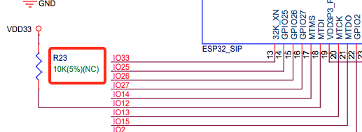
What does the term NC mean in Espressif schematics?
NC is the acronym of “No Component”. If you see a pull-up resistor is marked NC as shown in the figure below, it indicates that the component is not installed.
Does ESP32-C3F SPI CS0 pin need an external 10 kΩ pull-up resistor?
The SPI controller of ESP32-C3F supports software-programmable CS (Chip Select) pin without external 10 kΩ pull-up resistor.
- In ESP32-C3F, the CS pin can be set to any GPIO pin via SPI controller configuration. The GPIO state can be set in the code to control the level of the CS pin. When the SPI bus is idle, the CS pin is automatically pulled up to the default state of the GPIO pin without an external pull-up resistor.
Please note that when using a software-programmable CS pin, to select the target device, the pin should be manually pulled down before the SPI bus transmission. After the transmission is completed, pull the CS pin high to release the device. Additionally, the level and status of the CS pin should be adjusted according to the actual situation to ensure the stability and reliability of the SPI bus.
Is there any hardware design reference for ESP-Skainet Speech Recognition?
Is it necessary to connect a 32 kHz RTC crystal to the ESP32 chip in hardware design?
An external 32 kHz RTC crystal is optional, not mandatory. Its main purpose is to provide higher time accuracy and reduce power consumption. Typical application scenarios include:
Low Power Bluetooth (BLE) Design: An external 32 kHz crystal is mainly used for timing during BLE Light-sleep. If a 32 kHz external crystal is not added to the hardware, Light-sleep may not function correctly in some BLE applications.
Improved time accuracy: Compared with the internal RC oscillator, an external crystal oscillator is less affected by the environment and has higher accuracy. This is crucial for applications that require periodic wakeups to receive beacons (such as Wi-Fi/Bluetooth keep-alive), as it helps prevent RF receive windows from being extended due to clock drift, thereby significantly reducing average power consumption.
If the application scenario does not involve low power mode or there is no need to maintain high precision timing during sleep, the external crystal can be omitted.
The ESP32 integrates a 150 kHz RC oscillator and a clock derived from an 8.5 MHz oscillator divider, which can serve as RTC clock sources. Although their frequency stability is more sensitive to temperature variations, they can replace the external 32 kHz crystal oscillator in applications that do not have strict accuracy requirements.
For the ESP32-MINI-1 module, is there a component library for Altium Designer?
Our hardware schematics are developed with PADS. To find the .asc file that can be converted and opened in Altium Designer, please go to ESP32-MINI-1 Reference Design.
For hardware reference designs of other modules, please refer to technical documents.
Can I change the input voltage of UART0 of ESP8266 from 3.3 V to 1.8 V?
Yes. VDDPST is the power domain for UART0, the input voltage of which can be 1.8 V theoretically.
Is the level of UART0 of ESP8266 determined by VDD (VCC_WIFI) or VDDPST (VCC_CODEC_IO)?
The digital power voltage is determined by VDDPST, so the level of UART0 of ESP8266 is determined by VDDPST (hardware power domain).
What should be noted when I connect an external PSRAM to ESP32-D2WD?
Please enable CPUfrequece240Mhz and RTCclock80Mhz as follows:
When the VDD power supply of ESP32 slowly rises from 0 V to 3.3 V, why does the chip not start as usual?
This problem occurs because the power-on sequence requirements are not met. To start the chip, when VDD reaches 2.3 V, the EN voltage should not exceed 0.6 V.
If the VDD rise time is too long, the RC circuit on the EN side of the chip will not be able to delay EN.
You may modify the RC circuit, for example, increase the capacitance, adjust the resistance, or use the Reset chip to control EN state.
When the voltage provided to ESP32 is detected to be less than 2.3 V, you are recommended to pull down the EN pin of ESP32.
For ESP32 power-on sequence description, please refer to ESP32 Datasheet.
When using the ESP32-WROOM-32D module, can I set GPIO12 for other uses?
GPIO12 is a strapping pin that controls the startup voltage of SPI flash. The SPI flash startup voltage of the ESP32-WROOM-32D module is 3.3 V, so GPIO12 needs to be pulled down during powering on.
If you need to set GPIO12 for other uses, please use the command espefuse.py set_flash_voltage 3.3v in the esptool to set the voltage through VDD_SDIO as 3.3 V.
It is possible to connect VDD_SDIO to 3.3 V in hardware directly without burning eFuse again.
In the mass production stage, you can also download the firmware directly by modifying the default configuration of ESP32_EFUSE_CONFIG to config_voltage=3.3V in config/esp32/utility.config in the flash download tool.
When connecting an external flash to ESP32-WROOM-32D module, is it possible if I do not use GPIO6 ~ GPIO11 pins?
ESP32 has three sets of SPIs (SPI, HSPI, and VSPI), which can access the external flash through the SPI0/1(HSPI/VSPI) bus. The external flash connected to other pins (pins other than GPIO6 ~ GPIO11) can only receive data for storage, but not run code. If you need to run code from flash, please connect the flash to GPIO6 ~ GPIO11 pins only.
Do I need to add a shielding case to the PCB of ESP32 modules?
Whether a shield needs to be added depends on the specific application scenarios and requirements.
In some demanding application scenarios, such as severe wireless communication interference environments, high electromagnetic compatibility (EMC) test requirements, etc., installing a shield can effectively reduce external interference and mutual interference on the PCB board, improving the system’s stability and reliability. At this time, the shield should be made of conductive material and grounded to ensure its effectiveness.
On the other hand, if the application scenario is relatively simple, such as low wireless communication interference and low EMC requirements, the effect of adding a shield may not be very obvious and may increase system cost and complexity.
If the board has other signal interference, such as 2G, 3G, 4G, Wi-Fi, Bluetooth, Zigbee, etc., it is recommended to add a shielding case.
Do I must use GPIO0, GPIO1, or GPIO3 of ESP32 as the I2S CLK pin?
The MCLK pin must use GPIO0, GPIO1, or GPIO3. The other clock pins can use any GPIOs. Note that GPIO0 is generally not recommended for other functions because it is a strapping pin.
Does the ESP32-U4WDH chip support external PSRAM chips?
The ESP32-U4WDH chip supports external PSRAM chips. However, only the ESP-PSRAMXXH chip released by Espressif is supported. Third-party PSRAM chips are not supported.
For hardware design, all the PSRAM pins except for the CS pin can be multiplexed with Flash. For more information, please refer to the ESP32 Hardware Design Guidelines.
Also, when designing the PCB, please make sure that the GND of the PSRAM to the GND of the ESP32-U4WDH is as short as possible; Otherwise, the signal quality may be affected.
Does ESP32 support connection to an external SD NAND flash chip (instead of the default NOR flash chip) via the SPI0/SPI1 interface for storing application firmware?
The ESP32 chip does not support external SD NAND Flash chips using the SPI0/SPI1 (connect the core Flash) interface.
If you want to store external data, it is recommended to use the SPI2, SPI3, or SDIO interface of ESP32 to connect to an external NAND SD chip.
SPI2 and SPI3 can be used via any GPIOs, while the SDIO interface can only be used via the specified interface. For more information, please refer to Section Peripheral Pin Configurations in the ESP32 Datasheet.
Does it support to connect a second PSRAM chip externally based on the ESP32-S3R8 chip?
No, it is not supported. The reasons are as follows:
The PSRAM chip is connected to the MSPI bus. There are only two CS signals from the MSPI peripheral, one is connected to the flash, another is connected to the PSRAM.
CPU accesses external memory via cache and MSPI. A GPSPI peripheral is not accessible cache.
Could you please provide the 3D model and Footprint files of the ESP32-S3-WROOM-1 module?
The 3D models and Footprint files for the modules are available under the espressif/kicad-libraries library.
Does ESP32/ESP32-S2/ESP32-C3/ESP32-S3 support powering the RTC power domain only to keep the chip working with low power consumption?
At the hardware level, the following measures can be taken to improve the EMC performance of the PCB board.
The EMC performance with a four-layer board design will be better than a two-layer board hardware design.
Add filtering circuits to the power supply circuit.
Add ESD or magnetic beads to the antenna circuit.
Add a zero-ohm series resistor to the SPI Flash communication lines to lower the driving current, reduce interference to RF, and adjust timing for better interference shielding.
ESP32-S3 already has the ADC calibrated in hardware on the chip. ESP32-S3 ADCs can be sensitive to noise, resulting in large differences in ADC readings. Depending on the usage scenario, you may need to connect a bypass capacitor (e.g. 100 nF ceramic capacitor) to the ADC input pads for minimizing noise. In addition, multi-sampling can be used to further mitigate the effects of noise.
How to design an automatic download circuit based on the ESP32 series chip?
You can refer to the hardware design of the automatic download circuit in the ESP32-DevKitC V4 schematic.
Which crystal oscillator should be used on the ESP8266 chip?
The ESP8266 chip requires the 26 MHz crystal oscillators to start the chip. The crystal precision should be ±10 PPM. For details, please refer to 《ESP8266 Hardware Design Guidelines》.
Do the ESP32-C2, ESP32-C3 and ESP32-C6 chips support external PSRAM chips?
ESP32-C2, ESP32-C3, and ESP32-C6 do not support external PSRAM chips. However, ESP32-C61 will support 2 MB PSRAM.
When the ESP32-C3 is powered by a battery, it may fail to start if the supply voltage gradually decreases, for example, when the battery is fully discharged and then recharged. In such cases, the solution could only be disconnecting the battery from the ESP32-C3 and reconnect a fully charged battery, or to connect a voltage regulator diode between the 3.3 V pin and the EN pin to ensure the chip starts properly. What is the root cause of this situation? Is there an optimal solution?
Root cause: When powering up and resetting the ESP32-C3 chip, the CHIP_EN pin needs to meet the power-up timing specifications outlined in the ESP32-C3 datasheet or ESP32-C3 hardware design guidelines. If the battery discharge and power-up process are relatively slow, ESP32-C3 may not be fully reset, resulting in certain units of the chip being in an uncertain state.
Solution: Currently, if using battery power or energy storage systems, this issue can be addressed by adjusting RC component values, using voltage divider circuits with two resistors, or using a reset IC, which is a more commonly used approach. For detailed information regarding RC component values and related resistors, please refer to ESP32-C3 Family Hardware Design Guidelines.
Does the 3x3 GND grid on the ESP32 series module need to be copper-plated?
It is recommended to plate copper on the 3x3 GND grid of the module.
Why does ESP32 fail to start upon first power-up, and it requires a reset to start normally?
Please check if the Boot pin is connected to a capacitor that is too large.
What could be the possible hardware-level reasons for the failure of Ethernet PHY initialization?
It is suggested to try to use a 0 Ω series resistor.
Ethernet PHY initialization is successful, but unable to obtain an IP, what could be the possible reasons at the hardware level?
Please check if there is a significant load on GPIO0, you can remove the additional circuit and test again.
What could be the reason that a PCB designed with the ESP32 chip can not connect to the router properly?
Please connect a 24 nH inductor in series on XTAL_P.
Please adjust the capacitors on both sides of the crystal oscillator according to these steps.
Is it possible to change the default power-up reset initial state of GPIO6 (JTAG pin MTCK) of ESP32-C6, which is input enabled and internal weak pull-up resistor enabled (IE & WPU), to input enable only (IE) by burning eFuse?
Yes. After setting EFUSE DIS_PAD_JTAG to 1, the power-up reset initial state of GPIO6 (JTAG pin MTCK) is changed to input enabled (IE). Please refer to Section 2.2 Pin Overview in ESP32-C6 Datasheet.
The EFUSE DIS_PAD_JTAG can be set to 1 using the espefuse.py burn_efuse DIS_PAD_JTAG command.
You can also add the following code to the application code to set EFUSE DIS_PAD_JTAG to 1:
Can the VBAT pin of ESP32-H2 be powered independently?
In theory, RTC is supported for power supply, but 3.3V is already connected inside the module, so this pin is actually not available.
Is ESP32-P4 VBAT (Backup Battery) now fully supported?
IDF has support for VBAT, please refer to the examples/lowpower/vbat example. The document under solution is outdated, please refer to the latest IDF document. VBAT power supply is only switched during deep sleep, and light sleep does not switch to VBAT power supply. In this case, a 32.768 kHz crystal oscillator must be externally attached.