MIPI-DSI (MIPI Display Serial Interface) is a high-speed serial interface standard developed by the MIPI Alliance, specifically designed for connecting processors and display devices. It features:
High-speed transmission: Each data channel can support transmission rates up to several Gbps
Low power consumption: Uses low-voltage differential signaling and enters low-power mode during idle or low-speed transmission
Pin reduction: Significantly reduces the number of signal lines compared to parallel RGB interfaces
Scalability: Supports 1 to 4 data channels
High compatibility: Supports various resolutions and display devices
Currently, ESP32-P4 chips feature MIPI-DSI interfaces, supporting 2-lane × 1.5Gbps and using Video mode for video stream output.
MIPI-DSI is a commonly used display interface standard for connecting processors and displays. It supports two main data transmission modes:
Command Mode
Video Mode
ESP32-P4 currently only supports Video mode for video stream output.
In Video Mode, the host transmits data in continuous video frames, strictly synchronized with the display’s refresh cycle (such as VSync). The display does not require frame buffer memory, simplifying hardware design. This mode is widely used for high-resolution, high-refresh-rate display scenarios.
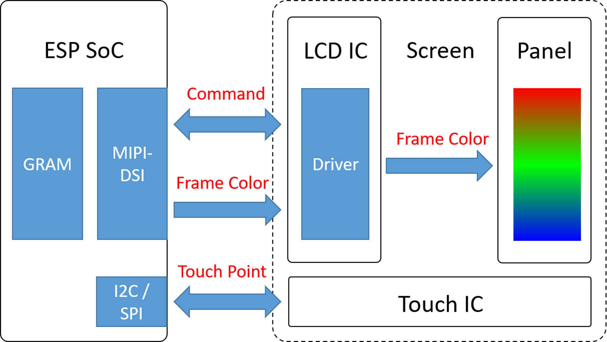
The figure above shows the MIPI-DSI screen refresh process, where:
Command data: MIPI-DCS commands are transmitted to the LCD controller through DBI for initializing registers and controlling display functions.
Frame color data: In MIPI-DSI Video mode, pixel data is continuously output from the host-side frame buffer (internal/external RAM) to the LCD panel for display through DMA, while the LCD driver IC does not require GRAM.
Touch data: Touch signals are detected by the touchscreen and transmitted back to the host system through I²C or SPI interfaces for processing.
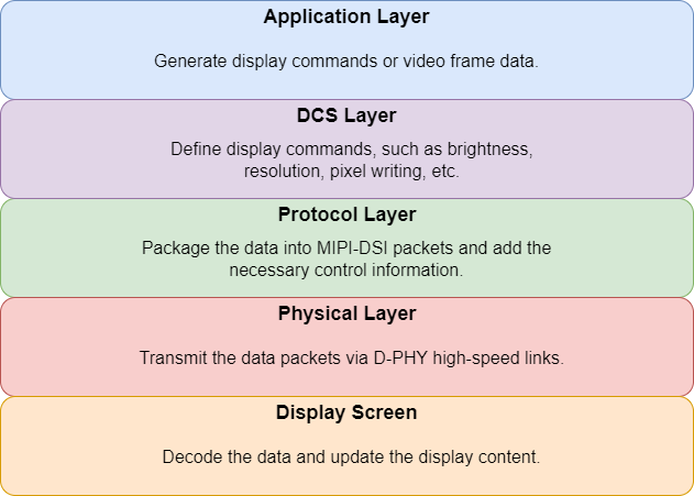
MIPI-DSI can be roughly divided into Physical Layer, Protocol Layer, and Display Command Layer (DCS Layer), each with specific functions that work together to complete command and pixel data transmission from the host to the display.
The collaborative workflow of each layer can be summarized as shown in the following figure:
Function: Responsible for actual data transmission, serving as the bottom layer of the protocol stack. Uses MIPI D-PHY to provide high-speed differential signal transmission, supporting multi-channel data transmission.
Transmission modes:
High-Speed Mode: Mainly used for transmitting display frame data, can also transmit commands, typically 80 Mbps ~ 1.5 Gbps/Lane.
Low-Power Mode: Typically used for sending DCS commands (in command mode) or controlling link states, maximum rate approximately 10 MHz (specific depends on chip support).
Configuration:
Clock Lane: Provides synchronization signals.
Data Lane: Transmits actual display data.
Detailed explanation of Lane Module, i.e., D-PHY:
Types
Lane Type/Transmission Role
Master
Slave
Unidirectional Clock Lane
HS-TX, LP-TX
HS-RX, LP-RX
Unidirectional Data Lane
HS-TX, LP-TX
HS-RX, LP-RX
Bidirectional Data Lane
HS-TX, LP-TX, HS-RX, LP-RX, LP-CD
HS-TX, LP-TX, HS-RX, LP-RX, LP-CD
Note
Module function descriptions:
LP-TX/LP-RX: Low-power transmitter/receiver
HS-TX/HS-RX: High-speed transmitter/receiver
LP-CD: Low-power contention detector
Clock lanes are typically unidirectional, provided by Master and received by Slave. Bidirectional lanes and LP-CD are mainly used for low-power communication in command mode.
States
LP States (LP-00, LP-01, LP-10, LP-11): Use single-ended signals, mainly for low-speed command transmission, control signals, initialization, or standby states. Different LP states are used for encoding and link control.
HS States (HS-0, HS-1): Use differential signals, mainly for high-speed transmission of video data or frame content. HS-0 and HS-1 correspond to logical levels on differential pairs, only valid on HS-TX/HS-RX.
Typical voltages
LP: Typical voltage approximately 0 – 1.2 V
HP: Typical differential voltage approximately 100 – 300 mV
Operation modes
Escape Mode: Only available in Low-Power Mode, MIPI-DSI’s low-power operation mode, used for special data transmission or triggering specific functions. Supports the following functions:
Function Name
Description
Command
LPDT (Low Power Data Transmission)
Transmit data in low-power mode
0x87
ULPS (Ultra Low Power State)
Enter ultra low power state for maximum energy savings
0x84
Trigger Command
Trigger specific events, such as state switching or mode adjustment
0x85
Entry process (signal state machine transition): LP-11 → LP-10 → LP-00 → LP-01 → LP-00
Exit process: LP-10 → LP-11
High-Speed (Burst) Mode: Always in High-Speed Mode, used for high-speed serial data transmission, suitable for high bandwidth requirements.
Entry process: LP-11 → LP-01 → LP-00 → SoT (Start of Transmission) → HSD (80Mbps ~ 1.5Gbps)
Exit process: EoT (End of Transmission) → LP-11
Control Mode: Default in Low-Power Mode, used for command transmission in stop state and bidirectional communication (BTA, Bus Turnaround).
Function: Implements data packaging and parsing, defines transmission formats (such as DCS and video data packets), and provides error detection mechanisms to ensure data correctness and reliability.
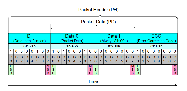
0x37: Data identifier, corresponding to DCS command “Set Maximum Return Packet Size”; Function: Set the maximum size of return data packets when the host receives data from the slave
0x03, 0x00: Frame data, indicating setting the maximum return packet size to 3 bytes
0x01: ECC (Error Correction Code)
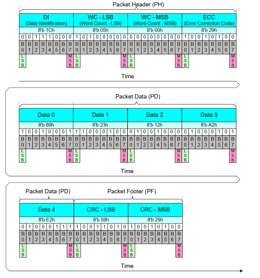
Long Packet:
Length: Variable length, 6 to 65541 bytes.
Composition: Frame header (Data Identifier (DI) 1 byte; Data Count (WC) 2 bytes; Error detection (ECC) 1 byte); Data payload (0 to 65535 bytes); Frame tail (Checksum 2 bytes).
Function: DCS (Display Command Set) is a standardized display command set defined by MIPI-DSI. The host interacts with the display through these commands to implement basic display module control (such as power on/off, sleep, backlight, display on/off), display parameter configuration (such as pixel format, display mode, address setting), and frame buffer access (such as writing image data, reading status information). DCS commands are transmitted on the DSI bus in the form of short write, long write, and read commands, serving as the main control interface between the application layer and display hardware.
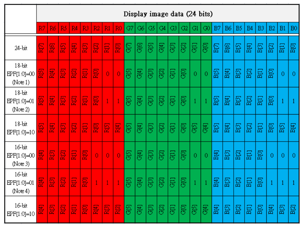
Most MIPI-DSI LCDs support multiple input color formats, such as RGB565, RGB666, RGB888.
The host can configure the display color depth through DCS command 0x3A (Pixel Format Set), for example:
When setting to RGB565 (16-bit), send Command:0x3A, Parameter:0x55 (specific parameter values need to refer to the LCD controller datasheet).
Pixel data is typically transmitted through Long Packets, which contain pixel data and corresponding Data Types.
For example, RGB565 format pixel streams generally use DT = 0x0E (Packed Pixel Stream, 16-bit).
The MIPI-DSI LCD driver flow can be roughly divided into four parts: initializing the DSI bus, configuring the DBI interface, porting the driver component, and initializing the LCD device.
esp_lcd_dsi_bus_handle_tdsi_bus=NULL;esp_lcd_dsi_bus_config_tbus_config={.bus_id=0,// DSI controller number.num_data_lanes=2,// Number of data lanes (1-2).phy_clk_src=MIPI_DSI_PHY_CLK_SRC_DEFAULT,// PHY clock source.lane_bit_rate_mbps=1300,// Bit rate per lane (Mbps)};ESP_ERROR_CHECK(esp_lcd_new_dsi_bus(&bus_config,&dsi_bus));
The number of data lanes (num_data_lanes) depends on the number of lanes used and supported by the LCD IC. Some LCD ICs can configure the number of lanes used through registers, while some LCD ICs have a fixed number of lanes. It’s worth noting that ESP32-P4 supports a maximum of 2 lanes, supporting both 1-lane and 2-lane LCD channel configurations.
Calculation method for bit rate per lane (lane_bit_rate_mbps):
Therefore, it is recommended to set lane_bit_rate_mbps to final_bit_rate, which is around 1300 in the example calculation scenario. Note that on the ESP32P4 platform, lane_bit_rate_mbps cannot exceed 1500, and the recommended minimum should not be below 480.
esp_lcd_panel_io_handle_tio_handle=NULL;esp_lcd_dbi_io_config_tio_config={.virtual_channel=0,// Virtual channel number (0-3), most LCDs only support channel `0`, usually set to `0`.lcd_cmd_bits=8,// Command bit width.lcd_param_bits=8,// Parameter bit width};ESP_ERROR_CHECK(esp_lcd_new_panel_io_dbi(dsi_bus,&io_config,&io_handle));
The command and parameter bit widths must match the panel specifications, and virtual channels are used to distinguish multiple devices.
The basic principles for porting MIPI-DSI LCD driver components include the following three points:
Send commands and parameters in specified formats based on interface device handles of type esp_lcd_panel_io_handle_t.
Implement and create an LCD device, then implement the functions in the esp_lcd_panel_t structure by registering callback functions.
Implement a function to provide LCD device handles of type esp_lcd_panel_handle_t, enabling applications to use LCD General APIs to operate the LCD device
Below is the implementation description of each function in esp_lcd_panel_handle_t and its correspondence with LCD General APIs:
For most MIPI-DSI LCDs, their driver IC commands and parameters are compatible with the implementation descriptions above, so porting can be completed through the following steps:
Select a MIPI-DSI LCD driver component with a similar model from LCD Driver Components.
Confirm whether the commands and parameters used in each function of the selected component are consistent with the target LCD driver IC by consulting the target LCD driver IC datasheet. If not, modify the relevant code.
Even for LCD driver ICs of the same model, screens from different manufacturers usually require their own initialization command configurations. Therefore, it is necessary to modify the commands and parameters sent in the initialization function init(). These initialization commands are usually stored in a static array in a specific format. Additionally, be careful not to include special commands in the initialization commands, such as LCD_CMD_COLMOD(3Ah) and LCD_CMD_MADCTL(36h), which are managed and used by the driver component.
Use the editor’s character search and replace function to replace the LCD driver IC name in the component with the target name, such as replacing ek79007 with ili9881
The following code example uses EK79007 as an example:
#include"esp_lcd_panel_vendor.h" // Required header file#include"esp_lcd_panel_ops.h"#include"esp_lcd_ek79007.h" // Target driver component header file// static const ek79007_lcd_init_cmd_t lcd_init_cmds[] = {// {cmd, { data }, data_size, delay_ms}// {0xE0, (uint8_t []){0x00}, 1, 0},// {0xE1, (uint8_t []){0x93}, 1, 0},// {0xE2, (uint8_t []){0x65}, 1, 0},// {0xE3, (uint8_t []){0xF8}, 1, 0},// ...// };ESP_LOGI(TAG,"MIPI DSI PHY Powered on");esp_ldo_channel_handle_tldo_mipi_phy=NULL;esp_ldo_channel_config_tldo_mipi_phy_config={.chan_id=3,.voltage_mv=2500,};ESP_ERROR_CHECK(esp_ldo_acquire_channel(&ldo_mipi_phy_config,&ldo_mipi_phy));ESP_LOGI(TAG,"Initialize MIPI DSI bus");esp_lcd_dsi_bus_handle_tmipi_dsi_bus=NULL;esp_lcd_dsi_bus_config_tbus_config=EK79007_PANEL_BUS_DSI_2CH_CONFIG();ESP_ERROR_CHECK(esp_lcd_new_dsi_bus(&bus_config,&mipi_dsi_bus));ESP_LOGI(TAG,"Install panel IO");esp_lcd_panel_io_handle_tmipi_dbi_io=NULL;esp_lcd_dpi_panel_config_tdpi_config={.virtual_channel=0,.dpi_clk_src=MIPI_DSI_DPI_CLK_SRC_DEFAULT,.dpi_clock_freq_mhz=60,// Pixel clock frequency.in_color_format=LCD_COLOR_FMT_RGB888,// Color format.video_timing={.h_size=800,// Horizontal resolution.v_size=1280,// Vertical resolution.hsync_pulse_width=4,// HSYNC pulse width.hsync_back_porch=20,// Horizontal back porch.hsync_front_porch=20,// Horizontal front porch.vsync_pulse_width=4,// VSYNC pulse width.vsync_back_porch=20,// Vertical back porch.vsync_front_porch=20,// Vertical front porch},.flags.use_dma2d=true,// Use 2D DMA acceleration};ESP_ERROR_CHECK(esp_lcd_new_panel_io_dbi(mipi_dsi_bus,&dbi_config,&mipi_dbi_io));ESP_LOGI(TAG,"Install EK79007S panel driver");esp_lcd_panel_handle_tpanel_handle=NULL;ek79007_vendor_config_tvendor_config={.flags={.use_mipi_interface=1,},.mipi_config={.dsi_bus=mipi_dsi_bus,.dpi_config=&dpi_config,},};constesp_lcd_panel_dev_config_tpanel_config={.reset_gpio_num=EXAMPLE_LCD_IO_RST,// Set to -1 if not use.rgb_ele_order=LCD_RGB_ELEMENT_ORDER_RGB,// Implemented by LCD command `36h`.bits_per_pixel=EXAMPLE_LCD_BIT_PER_PIXEL,// Implemented by LCD command `3Ah` (16/18/24).vendor_config=&vendor_config,};ESP_ERROR_CHECK(esp_lcd_new_panel_ek79007(mipi_dbi_io,&panel_config,&panel_handle));ESP_ERROR_CHECK(esp_lcd_panel_reset(panel_handle));ESP_ERROR_CHECK(esp_lcd_panel_init(panel_handle));ESP_ERROR_CHECK(esp_lcd_panel_disp_on_off(panel_handle,true));
Timing Parameter Description:
The timing parameter definitions for MIPI-DSI are consistent with the SYNC Mode of the RGB interface in terms of timing diagrams. Both use HSYNC and VSYNC synchronization signals and require configuration of blanking porch parameters. For detailed explanations of timing parameters, the correspondence between parameters and timing diagram symbols, and configuration methods, please refer to the “Timing Parameter Correspondence” section in RGB LCD Introduction.
Note that ESP32P4 requires a stable 2.5V power supply for the MIPI DSI PHY. The clock frequency calculation refers to the pixel_clock calculation method mentioned above. Color format, resolution, pulse width, and front/back porch parameters must strictly follow the panel datasheet requirements.
Then create an LCD device through the ported driver component and obtain a handle of type esp_lcd_panel_handle_t, then use LCD General APIs to initialize the LCD device.
For more detailed explanations of MIPI-DSI interface configuration parameters, please refer to the ESP-IDF Programming Guide. Below are some explanations about using the function esp_lcd_panel_draw_bitmap() to refresh LCD images:
This function refreshes image data in the frame buffer through memory copy, meaning that after the function call completes, the image data in the frame buffer has also been updated. The MIPI-DSI interface itself uses DMA to fetch image data from the frame buffer to refresh the LCD, and these two processes are asynchronous.
This function will check whether the incoming parameter color_data value is the internal frame buffer address of the MIPI-DSI interface. If so, it will not perform the above memory copy operation, but directly set the DMA transfer address of the MIPI-DSI interface to that buffer address, thus achieving switching functionality in cases with multiple frame buffers.
esp_lcd_dpi_panel_get_frame_buffer(): Get frame buffer addresses, available quantity determined by configuration parameter num_fbs, used for multi-buffer anti-tearing.
esp_lcd_dpi_panel_set_pattern(): Set predefined patterns to the screen for testing or debugging purposes.
esp_lcd_dpi_panel_set_yuv_conversion(): Set YUV conversion configuration for DPI panel.
esp_lcd_dpi_panel_register_event_callbacks(): Register callback functions for various events, example code and explanation as follows:
staticboolexample_on_color_trans_event(esp_lcd_panel_handle_tpanel,constesp_lcd_dpi_panel_event_callbacks_t*edata,void*user_ctx){/* Operations can be performed here */returnfalse;}staticboolexample_on_refresh_event(esp_lcd_panel_handle_tpanel,constesp_lcd_dpi_panel_event_callbacks_t*edata,void*user_ctx){/* Operations can be performed here */returnfalse;}esp_lcd_dpi_panel_event_callbacks_tcbs={.on_color_trans_done=example_on_color_trans_event,// Triggered when user's color buffer is copied to internal frame buffer.on_refresh_done=example_on_refresh_event,// Triggered when internal frame buffer content completes refresh and displays on screen};ESP_ERROR_CHECK(esp_lcd_dpi_panel_register_event_callbacks(panel_handle,&cbs,&example_user_ctx));
The chip’s DSI data pins (DSI_DATAN0 and DSI_DATAP0) and clock pins (DSI_CLKN and DSI_CLKP) are not correctly connected to the screen’s data pins and clock pins.
This situation is generally caused by mismatch between lane_bit_rate_mbps and pixel_clock, or mismatch between lane_bit_rate_mbps and screen required rate. You can adjust the lane_bit_rate_mbps value and test, specifically refer to the pixel_clock calculation method mentioned above.
This issue occurs due to insufficient PSRAM bandwidth. You can consider reducing lane_bit_rate_mbps and pixel_clock values. In RGB888 color format scenarios, you can consider changing to RGB565 format. Also consider configuring the following options to improve PSRAM bandwidth:
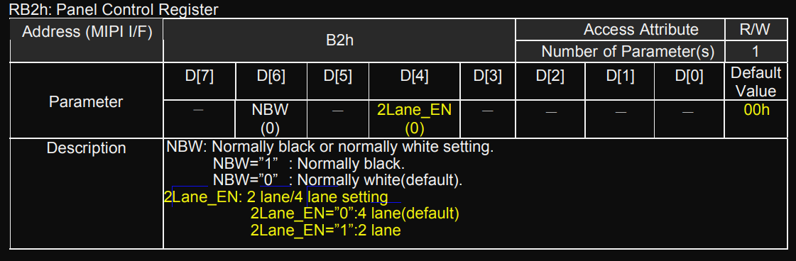
Most LCD ICs support adjusting the number of lanes through registers, but the register addresses and operations differ between ICs. You need to confirm whether the lane count can be adjusted based on the specific IC’s datasheet or directly consult the screen manufacturer. For example, in EK79007, you can configure the 0xB2 register to choose between 2-lane/4-lane.
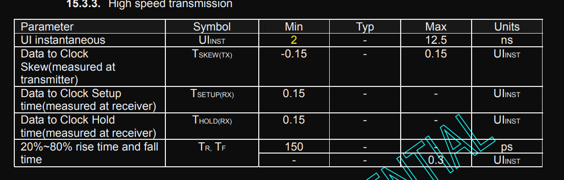
In high-speed serial communication, UI usually refers to the time unit of signal bits (bit) on the physical channel, which is one bit time (bit period). For example, if the frame rate or link rate is 1 Gbps, then one UI ≈ 1 nanosecond (ns). If the rate is 500 Mbps, then UI ≈ 2 ns, and so on. Therefore, you can calculate the lane bit rate range based on the AC ELECTRICAL CHARACTERISTIC - High speed transmission in the LCD IC datasheet. As shown in the figure, the lane bit rate (transmission rate of a single Data Lane) ranges from 20Mbps to 500Mbps.