SPI Master Driver
SPI Master driver is a program that controls ESP32’s SPI peripherals while they function as masters.
Overview of ESP32’s SPI peripherals
ESP32 integrates four SPI peripherals.
SPI0 and SPI1 are used internally to access the ESP32’s attached flash memory and share an arbiter.
There are quite a few limitations when using SPI Master driver on the SPI1 bus, see Notes on Using the SPI Master driver on SPI1 Bus.
SPI2 and SPI3 are general purpose SPI controllers, sometimes referred to as HSPI and VSPI, respectively. They are open to users. SPI2 and SPI3 have independent signal buses with the same respective names. Each bus has three CS lines to drive up to three SPI slaves.
Terminology
The terms used in relation to the SPI master driver are given in the table below.
Term |
Definition |
|---|---|
Host |
The SPI controller peripheral inside ESP32 that initiates SPI transmissions over the bus, and acts as an SPI Master. This may be the SPI2 or SPI3 peripheral. (The driver will also support the SPI1 peripheral in the future.) |
Device |
SPI slave device. An SPI bus may be connected to one or more Devices. Each Device shares the MOSI, MISO and SCLK signals but is only active on the bus when the Host asserts the Device’s individual CS line. |
Bus |
A signal bus, common to all Devices connected to one Host. In general, a bus includes the following lines: MISO, MOSI, SCLK, one or more CS lines, and, optionally, QUADWP and QUADHD. So Devices are connected to the same lines, with the exception that each Device has its own CS line. Several Devices can also share one CS line if connected in the daisy-chain manner. |
|
Master In, Slave Out, a.k.a. Q. Data transmission from a Device to Host. |
|
Master Out, Slave In, a.k.a. D. Data transmission from a Host to Device. |
|
Serial Clock. Oscillating signal generated by a Host that keeps the transmission of data bits in sync. |
|
Chip Select. Allows a Host to select individual Device(s) connected to the bus in order to send or receive data. |
|
Write Protect signal. Only used for 4-bit (qio/qout) transactions. |
|
Hold signal. Only used for 4-bit (qio/qout) transactions. |
|
The action of activating a line. The opposite action of returning the line back to inactive (back to idle) is called de-assertion. |
Transaction |
One instance of a Host asserting a CS line, transferring data to and from a Device, and de-asserting the CS line. Transactions are atomic, which means they can never be interrupted by another transaction. |
Launch edge |
Edge of the clock at which the source register launches the signal onto the line. |
Latch edge |
Edge of the clock at which the destination register latches in the signal. |
Driver Features
The SPI master driver governs communications of Hosts with Devices. The driver supports the following features:
Multi-threaded environments
Transparent handling of DMA transfers while reading and writing data
Automatic time-division multiplexing of data coming from different Devices on the same signal bus, see SPI Bus Lock.
警告
The SPI master driver has the concept of multiple Devices connected to a single bus (sharing a single ESP32 SPI peripheral). As long as each Device is accessed by only one task, the driver is thread safe. However, if multiple tasks try to access the same SPI Device, the driver is not thread-safe. In this case, it is recommended to either:
Refactor your application so that each SPI peripheral is only accessed by a single task at a time.
Add a mutex lock around the shared Device using
xSemaphoreCreateMutex.
SPI Transactions
An SPI bus transaction consists of five phases which can be found in the table below. Any of these phases can be skipped.
Phase |
Description |
|---|---|
Command |
In this phase, a command (0-16 bit) is written to the bus by the Host. |
Address |
In this phase, an address (0-64 bit) is transmitted over the bus by the Host. |
Write |
Host sends data to a Device. This data follows the optional command and address phases and is indistinguishable from them at the electrical level. |
Dummy |
This phase is configurable and is used to meet the timing requirements. |
Read |
Device sends data to its Host. |
The attributes of a transaction are determined by the bus configuration structure spi_bus_config_t, device configuration structure spi_device_interface_config_t, and transaction configuration structure spi_transaction_t.
An SPI Host can send full-duplex transactions, during which the read and write phases occur simultaneously. The total transaction length is determined by the sum of the following members:
While the member spi_transaction_t::rxlength only determines the length of data received into the buffer.
In half-duplex transactions, the read and write phases are not simultaneous (one direction at a time). The lengths of the write and read phases are determined by length and rxlength members of the struct spi_transaction_t respectively.
The command and address phases are optional, as not every SPI device requires a command and/or address. This is reflected in the Device’s configuration: if command_bits and/or address_bits are set to zero, no command or address phase will occur.
The read and write phases can also be optional, as not every transaction requires both writing and reading data. If rx_buffer is NULL and SPI_TRANS_USE_RXDATA is not set, the read phase is skipped. If tx_buffer is NULL and SPI_TRANS_USE_TXDATA is not set, the write phase is skipped.
The driver supports two types of transactions: the interrupt transactions and polling transactions. The programmer can choose to use a different transaction type per Device. If your Device requires both transaction types, see Notes on Sending Mixed Transactions to the Same Device.
Interrupt Transactions
Interrupt transactions will block the transaction routine until the transaction completes, thus allowing the CPU to run other tasks.
An application task can queue multiple transactions, and the driver will automatically handle them one-by-one in the interrupt service routine (ISR). It allows the task to switch to other procedures until all the transactions complete.
Polling Transactions
Polling transactions do not use interrupts. The routine keeps polling the SPI Host’s status bit until the transaction is finished.
All the tasks that use interrupt transactions can be blocked by the queue. At this point, they will need to wait for the ISR to run twice before the transaction is finished. Polling transactions save time otherwise spent on queue handling and context switching, which results in smaller transaction intervals. The disadvantage is that the CPU is busy while these transactions are in progress.
The spi_device_polling_end() routine needs an overhead of at least 1 us to unblock other tasks when the transaction is finished. It is strongly recommended to wrap a series of polling transactions using the functions spi_device_acquire_bus() and spi_device_release_bus() to avoid the overhead. For more information, see Bus Acquiring.
Command and Address Phases
During the command and address phases, the members cmd and addr in the struct spi_transaction_t are sent to the bus, nothing is read at this time. The default lengths of the command and address phases are set in spi_device_interface_config_t by calling spi_bus_add_device(). If the flags SPI_TRANS_VARIABLE_CMD and SPI_TRANS_VARIABLE_ADDR in the member spi_transaction_t::flags are not set, the driver automatically sets the length of these phases to default values during Device initialization.
If the lengths of the command and address phases need to be variable, declare the struct spi_transaction_ext_t, set the flags SPI_TRANS_VARIABLE_CMD and/or SPI_TRANS_VARIABLE_ADDR in the member spi_transaction_ext_t::base and configure the rest of base as usual. Then the length of each phase will be equal to command_bits and address_bits set in the struct spi_transaction_ext_t.
Write and Read Phases
Normally, the data that needs to be transferred to or from a Device will be read from or written to a chunk of memory indicated by the members rx_buffer and tx_buffer of the structure spi_transaction_t. If DMA is enabled for transfers, the buffers are required to be:
Allocated in DMA-capable internal memory. If external PSRAM is enabled, this means using
pvPortMallocCaps(size, MALLOC_CAP_DMA).32-bit aligned (staring from a 32-bit boundary and having a length of multiples of 4 bytes).
If these requirements are not satisfied, the transaction efficiency will be affected due to the allocation and copying of temporary buffers.
注解
Half-duplex transactions with both read and write phases are not supported when using DMA. For details and workarounds, see Known Issues.
Bus Acquiring
Sometimes you might want to send SPI transactions exclusively and continuously so that it takes as little time as possible. For this, you can use bus acquiring, which helps to suspend transactions (both polling or interrupt) to other devices until the bus is released. To acquire and release a bus, use the functions spi_device_acquire_bus() and spi_device_release_bus().
Driver Usage
Initialize an SPI bus by calling the function
spi_bus_initialize(). Make sure to set the correct I/O pins in the structspi_bus_config_t. Set the signals that are not needed to-1.Register a Device connected to the bus with the driver by calling the function
spi_bus_add_device(). Make sure to configure any timing requirements the device might need with the parameterdev_config. You should now have obtained the Device’s handle which will be used when sending a transaction to it.To interact with the Device, fill one or more
spi_transaction_tstructs with any transaction parameters required. Then send the structs either using a polling transaction or an interrupt transaction:- Interrupt
Either queue all transactions by calling the function
spi_device_queue_trans()and, at a later time, query the result using the functionspi_device_get_trans_result(), or handle all requests synchronously by feeding them intospi_device_transmit().
- Polling
Call the function
spi_device_polling_transmit()to send polling transactions. Alternatively, if you want to insert something in between, send the transactions by usingspi_device_polling_start()andspi_device_polling_end().
(Optional) To perform back-to-back transactions with a Device, call the function
spi_device_acquire_bus()before sending transactions andspi_device_release_bus()after the transactions have been sent.(Optional) To unload the driver for a certain Device, call
spi_bus_remove_device()with the Device handle as an argument.(Optional) To remove the driver for a bus, make sure no more drivers are attached and call
spi_bus_free().
The example code for the SPI master driver can be found in the peripherals/spi_master directory of ESP-IDF examples.
Transactions with Data Not Exceeding 32 Bits
When the transaction data size is equal to or less than 32 bits, it will be sub-optimal to allocate a buffer for the data. The data can be directly stored in the transaction struct instead. For transmitted data, it can be achieved by using the tx_data member and setting the SPI_TRANS_USE_TXDATA flag on the transmission. For received data, use rx_data and set SPI_TRANS_USE_RXDATA. In both cases, do not touch the tx_buffer or rx_buffer members, because they use the same memory locations as tx_data and rx_data.
Transactions with Integers Other Than uint8_t
An SPI Host reads and writes data into memory byte by byte. By default, data is sent with the most significant bit (MSB) first, as LSB first used in rare cases. If a value less than 8 bits needs to be sent, the bits should be written into memory in the MSB first manner.
For example, if 0b00010 needs to be sent, it should be written into a uint8_t variable, and the length for reading should be set to 5 bits. The Device will still receive 8 bits with 3 additional “random” bits, so the reading must be performed correctly.
On top of that, ESP32 is a little-endian chip, which means that the least significant byte of uint16_t and uint32_t variables is stored at the smallest address. Hence, if uint16_t is stored in memory, bits [7:0] are sent first, followed by bits [15:8].
For cases when the data to be transmitted has the size differing from uint8_t arrays, the following macros can be used to transform data to the format that can be sent by the SPI driver directly:
SPI_SWAP_DATA_TXfor data to be transmittedSPI_SWAP_DATA_RXfor data received
Notes on Sending Mixed Transactions to the Same Device
To reduce coding complexity, send only one type of transactions (interrupt or polling) to one Device. However, you still can send both interrupt and polling transactions alternately. The notes below explain how to do this.
The polling transactions should be initiated only after all the polling and interrupt transactions are finished.
Since an unfinished polling transaction blocks other transactions, please do not forget to call the function spi_device_polling_end() after spi_device_polling_start() to allow other transactions or to allow other Devices to use the bus. Remember that if there is no need to switch to other tasks during your polling transaction, you can initiate a transaction with spi_device_polling_transmit() so that it will be ended automatically.
In-flight polling transactions are disturbed by the ISR operation to accommodate interrupt transactions. Always make sure that all the interrupt transactions sent to the ISR are finished before you call spi_device_polling_start(). To do that, you can keep calling spi_device_get_trans_result() until all the transactions are returned.
To have better control of the calling sequence of functions, send mixed transactions to the same Device only within a single task.
Notes on Using the SPI Master driver on SPI1 Bus
注解
Though the SPI Bus Lock feature makes it possible to use SPI Master driver on the SPI1 bus, it’s still tricky and needs a lot of special treatment. It’s a feature for advanced developers.
To use SPI Master driver on SPI1 bus, you have to take care of two problems:
The code and data, required at the meanwhile the driver is operating SPI1 bus, should be in the internal memory.
SPI1 bus is shared among devices and the cache for data (code) in the Flash as well as the PSRAM. The cache should be disabled during the other drivers are operating the SPI1 bus. Hence the data (code) in the flash as well as the PSRAM cannot be fetched at the meanwhile the driver acquires the SPI1 bus by:
Explicit bus acquiring between
spi_device_acquire_bus()andspi_device_release_bus().Implicit bus acquiring between
spi_device_polling_start()andspi_device_polling_end()(or insidespi_device_polling_transmit()).
During the time above, all other tasks and most ISRs will be disabled (see IRAM 安全中断处理程序). Application code and data used by current task should be placed in internal memory (DRAM or IRAM), or already in the ROM. Access to external memory (flash code, const data in the flash, and static/heap data in the PSRAM) will cause a Cache disabled but cached memory region accessed exception. For differences between IRAM, DRAM, and flash cache, please refer to the application memory layout documentation.
To place functions into the IRAM, you can either:
Add IRAM_ATTR (include “esp_attr.h”) to the function like:
IRAM_ATTR void foo(void) { }
Please note that when a function is inlined, it will follow its caller’s segment, and the attribute will not take effect. You may need to use NOLINE_ATTR to avoid this.
Use the noflash placement in the linker.lf. See more in 链接脚本生成机制. Please note that, some code may be transformed into lookup table in the const data by the compiler, so noflash_text is not safe.
Please do take care that the optimization level may affect the compiler behavior of inline, or transforming some code into lookup table in the const data, etc.
To place data into the DRAM, you can either:
Add DRAM_ATTR (include “esp_attr.h”) to the data definition like:
DRAM_ATTR int g_foo = 3;
Use the noflash placement in the linker.lf. See more in 链接脚本生成机制.
Please also see the example peripherals/spi_master/hd_eeprom.
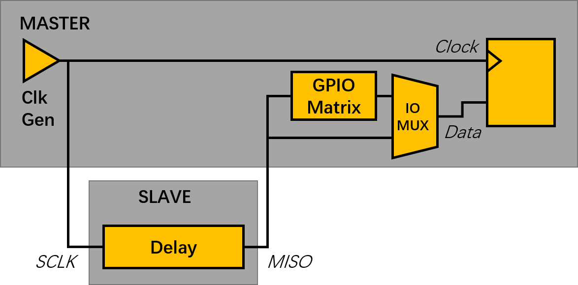
GPIO Matrix and IO_MUX
Most of ESP32’s peripheral signals have direct connection to their dedicated IO_MUX pins. However, the signals can also be routed to any other available pins using the less direct GPIO matrix. If at least one signal is routed through the GPIO matrix, then all signals will be routed through it.
The GPIO matrix introduces flexibility of routing but also brings the following disadvantages:
Increases the input delay of the MISO signal, which makes MISO setup time violations more likely. If SPI needs to operate at high speeds, use dedicated IO_MUX pins.
Allows signals with clock frequencies only up to 40 MHz, as opposed to 80 MHz if IO_MUX pins are used.
注解
For more details about the influence of the MISO input delay on the maximum clock frequency, see Timing Considerations.
The IO_MUX pins for SPI buses are given below.
Pin Name |
SPI2 |
SPI3 |
|---|---|---|
GPIO Number |
||
CS0* |
15 |
5 |
SCLK |
14 |
18 |
MISO |
12 |
19 |
MOSI |
13 |
23 |
QUADWP |
2 |
22 |
QUADHD |
4 |
21 |
Only the first Device attached to the bus can use the CS0 pin.
Transfer Speed Considerations
There are three factors limiting the transfer speed:
Transaction interval
SPI clock frequency
Cache miss of SPI functions, including callbacks
The main parameter that determines the transfer speed for large transactions is clock frequency. For multiple small transactions, the transfer speed is mostly determined by the length of transaction intervals.
Transaction Interval
Transaction interval is the time that software requires to set up SPI peripheral registers and to copy data to FIFOs, or to set up DMA links.
Interrupt transactions allow appending extra overhead to accommodate the cost of FreeRTOS queues and the time needed for switching between tasks and the ISR.
For interrupt transactions, the CPU can switch to other tasks when a transaction is in progress. This saves the CPU time but increases the interval. See Interrupt Transactions. For polling transactions, it does not block the task but allows to do polling when the transaction is in progress. For more information, see Polling Transactions.
If DMA is enabled, setting up the linked list requires about 2 us per transaction. When a master is transferring data, it automatically reads the data from the linked list. If DMA is not enabled, the CPU has to write and read each byte from the FIFO by itself. Usually, this is faster than 2 us, but the transaction length is limited to 64 bytes for both write and read.
Typical transaction interval timings for one byte of data are given below.
Typical Transaction Time (us) |
||
|---|---|---|
Interrupt |
Polling |
|
DMA |
24 |
8 |
No DMA |
22 |
7 |
SPI Clock Frequency
Transferring each byte takes eight times the clock period 8/fspi. If the clock frequency is too high, the use of some functions might be limited. See Timing Considerations.
Cache Miss
The default config puts only the ISR into the IRAM. Other SPI related functions, including the driver itself and the callback, might suffer from the cache miss and will need to wait until the code is read from the flash. Select CONFIG_SPI_MASTER_IN_IRAM to put the whole SPI driver into IRAM and put the entire callback(s) and its callee functions into IRAM to prevent cache miss.
For an interrupt transaction, the overall cost is 20+8n/Fspi[MHz] [us] for n bytes transferred in one transaction. Hence, the transferring speed is: n/(20+8n/Fspi). An example of transferring speed at 8 MHz clock speed is given in the following table.
Frequency (MHz) |
Transaction Interval (us) |
Transaction Length (bytes) |
Total Time (us) |
Total Speed (KBps) |
|---|---|---|---|---|
8 |
25 |
1 |
26 |
38.5 |
8 |
25 |
8 |
33 |
242.4 |
8 |
25 |
16 |
41 |
490.2 |
8 |
25 |
64 |
89 |
719.1 |
8 |
25 |
128 |
153 |
836.6 |
When a transaction length is short, the cost of transaction interval is high. If possible, try to squash several short transactions into one transaction to achieve a higher transfer speed.
Please note that the ISR is disabled during flash operation by default. To keep sending transactions during flash operations, enable CONFIG_SPI_MASTER_ISR_IN_IRAM and set ESP_INTR_FLAG_IRAM in the member spi_bus_config_t::intr_flags. In this case, all the transactions queued before starting flash operations will be handled by the ISR in parallel. Also note that the callback of each Device and their callee functions should be in IRAM, or your callback will crash due to cache miss. For more details, see IRAM 安全中断处理程序.
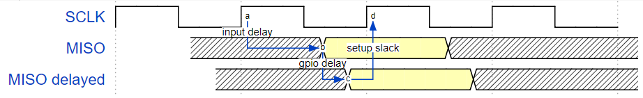
Timing Considerations
As shown in the figure below, there is a delay on the MISO line after the SCLK launch edge and before the signal is latched by the internal register. As a result, the MISO pin setup time is the limiting factor for the SPI clock speed. When the delay is too long, the setup slack is < 0, and the setup timing requirement is violated, which results in the failure to perform the reading correctly.
The maximum allowed frequency is dependent on:
input_delay_ns- maximum data valid time on the MISO bus after a clock cycle on SCLK startsIf the IO_MUX pin or the GPIO Matrix is used
When the GPIO matrix is used, the maximum allowed frequency is reduced to about 33~77% in comparison to the existing input delay. To retain a higher frequency, you have to use the IO_MUX pins or the dummy bit workaround. You can obtain the maximum reading frequency of the master by using the function spi_get_freq_limit().
Dummy bit workaround: Dummy clocks, during which the Host does not read data, can be inserted before the read phase begins. The Device still sees the dummy clocks and sends out data, but the Host does not read until the read phase comes. This compensates for the lack of the MISO setup time required by the Host and allows the Host to do reading at a higher frequency.
In the ideal case, if the Device is so fast that the input delay is shorter than an APB clock cycle - 12.5 ns - the maximum frequency at which the Host can read (or read and write) in different conditions is as follows:
Frequency Limit (MHz) |
Dummy Bits Used By Driver |
Comments |
|
|---|---|---|---|
GPIO matrix |
IO_MUX pins |
||
26.6 |
80 |
No |
|
40 |
– |
Yes |
Half-duplex, no DMA allowed |
If the Host only writes data, the dummy bit workaround and the frequency check can be disabled by setting the bit SPI_DEVICE_NO_DUMMY in the member spi_device_interface_config_t::flags. When disabled, the output frequency can be 80MHz, even if the GPIO matrix is used.
spi_device_interface_config_t::flags
The SPI master driver can work even if the input_delay_ns in the structure spi_device_interface_config_t is set to 0. However, setting an accurate value helps to:
Calculate the frequency limit for full-duplex transactions
Compensate the timing correctly with dummy bits for half-duplex transactions
You can approximate the maximum data valid time after the launch edge of SPI clocks by checking the statistics in the AC characteristics chapter of your Device’s specification or measure the time on an oscilloscope or logic analyzer.
Please note that the actual PCB layout design and the excessive loads may increase the input delay. It means that non-optimal wiring and/or a load capacitor on the bus will most likely lead to the input delay values exceeding the values given in the Device specification or measured while the bus is floating.
Some typical delay values are shown in the following table.
Device |
Input delay (ns) |
|---|---|
Ideal Device |
0 |
ESP32 slave using IO_MUX* |
50 |
ESP32 slave using GPIO_MUX* |
75 |
ESP32’s slave device is on a different physical chip. |
|
The MISO path delay (valid time) consists of a slave’s input delay plus master’s GPIO matrix delay. This delay determines the frequency limit above which full-duplex transfers will not work as well as the dummy bits used in the half-duplex transactions. The frequency limit is:
Freq limit [MHz] = 80 / (floor(MISO delay[ns]/12.5) + 1)
The figure below shows the relationship between frequency limit and input delay. Two extra APB clock cycle periods should be added to the MISO delay if the master uses the GPIO matrix.
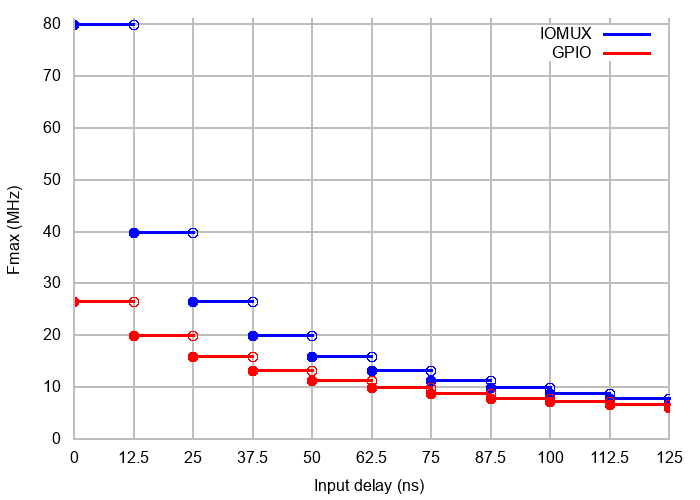
Corresponding frequency limits for different Devices with different input delay times are shown in the table below.
Master |
Input delay (ns) |
MISO path delay (ns) |
Freq. limit (MHz) |
|---|---|---|---|
IO_MUX (0ns) |
0 |
0 |
80 |
50 |
50 |
16 |
|
75 |
75 |
11.43 |
|
GPIO (25ns) |
0 |
25 |
26.67 |
50 |
75 |
11.43 |
|
75 |
100 |
8.89 |
Known Issues
Half-duplex transactions are not compatible with DMA when both writing and reading phases are used.
If such transactions are required, you have to use one of the alternative solutions:
Use full-duplex transactions instead.
- Disable DMA by setting the bus initialization function’s last parameter to 0 as follows:
ret=spi_bus_initialize(VSPI_HOST, &buscfg, 0);
This can prohibit you from transmitting and receiving data longer than 64 bytes. 3. Try using the command and address fields to replace the write phase.
2. Full-duplex transactions are not compatible with the dummy bit workaround, hence the frequency is limited. See dummy bit speed-up workaround.
cs_ena_pretransis not compatible with the command and address phases of full-duplex transactions.
Application Example
The code example for displaying graphics on an ESP32-WROVER-KIT’s 320x240 LCD screen can be found in the peripherals/spi_master directory of ESP-IDF examples.
API Reference - SPI Common
Header File
Enumerations
Header File
Functions
-
esp_err_t
spi_bus_initialize(spi_host_device_t host_id, const spi_bus_config_t *bus_config, int dma_chan)¶ Initialize a SPI bus.
- Warning
For now, only supports HSPI and VSPI.
- Warning
If a DMA channel is selected, any transmit and receive buffer used should be allocated in DMA-capable memory.
- Warning
The ISR of SPI is always executed on the core which calls this function. Never starve the ISR on this core or the SPI transactions will not be handled.
- Return
ESP_ERR_INVALID_ARG if configuration is invalid
ESP_ERR_INVALID_STATE if host already is in use
ESP_ERR_NO_MEM if out of memory
ESP_OK on success
- Parameters
host_id: SPI peripheral that controls this busbus_config: Pointer to a spi_bus_config_t struct specifying how the host should be initializeddma_chan: Either channel 1 or 2, or 0 in the case when no DMA is required. Selecting a DMA channel for a SPI bus allows transfers on the bus to have sizes only limited by the amount of internal memory. Selecting no DMA channel (by passing the value 0) limits the amount of bytes transfered to a maximum of 64. Set to 0 if only the SPI flash uses this bus.
-
esp_err_t
spi_bus_free(spi_host_device_t host_id)¶ Free a SPI bus.
- Warning
In order for this to succeed, all devices have to be removed first.
- Return
ESP_ERR_INVALID_ARG if parameter is invalid
ESP_ERR_INVALID_STATE if bus hasn’t been initialized before, or not all devices on the bus are freed
ESP_OK on success
- Parameters
host_id: SPI peripheral to free
Structures
-
struct
spi_bus_config_t¶ This is a configuration structure for a SPI bus.
You can use this structure to specify the GPIO pins of the bus. Normally, the driver will use the GPIO matrix to route the signals. An exception is made when all signals either can be routed through the IO_MUX or are -1. In that case, the IO_MUX is used, allowing for >40MHz speeds.
- Note
Be advised that the slave driver does not use the quadwp/quadhd lines and fields in spi_bus_config_t refering to these lines will be ignored and can thus safely be left uninitialized.
Public Members
-
int
mosi_io_num¶ GPIO pin for Master Out Slave In (=spi_d) signal, or -1 if not used.
-
int
miso_io_num¶ GPIO pin for Master In Slave Out (=spi_q) signal, or -1 if not used.
-
int
sclk_io_num¶ GPIO pin for Spi CLocK signal, or -1 if not used.
-
int
quadwp_io_num¶ GPIO pin for WP (Write Protect) signal which is used as D2 in 4-bit communication modes, or -1 if not used.
-
int
quadhd_io_num¶ GPIO pin for HD (HolD) signal which is used as D3 in 4-bit communication modes, or -1 if not used.
-
int
max_transfer_sz¶ Maximum transfer size, in bytes. Defaults to 4092 if 0 when DMA enabled, or to
SOC_SPI_MAXIMUM_BUFFER_SIZEif DMA is disabled.
-
uint32_t
flags¶ Abilities of bus to be checked by the driver. Or-ed value of
SPICOMMON_BUSFLAG_*flags.
-
int
intr_flags¶ Interrupt flag for the bus to set the priority, and IRAM attribute, see
esp_intr_alloc.h. Note that the EDGE, INTRDISABLED attribute are ignored by the driver. Note that if ESP_INTR_FLAG_IRAM is set, ALL the callbacks of the driver, and their callee functions, should be put in the IRAM.
Macros
-
SPI_MAX_DMA_LEN
-
SPI_SWAP_DATA_TX(DATA, LEN)¶ Transform unsigned integer of length <= 32 bits to the format which can be sent by the SPI driver directly.
E.g. to send 9 bits of data, you can:
uint16_t data = SPI_SWAP_DATA_TX(0x145, 9);
Then points tx_buffer to
&data.- Parameters
DATA: Data to be sent, can be uint8_t, uint16_t or uint32_t.LEN: Length of data to be sent, since the SPI peripheral sends from the MSB, this helps to shift the data to the MSB.
-
SPI_SWAP_DATA_RX(DATA, LEN)¶ Transform received data of length <= 32 bits to the format of an unsigned integer.
E.g. to transform the data of 15 bits placed in a 4-byte array to integer:
uint16_t data = SPI_SWAP_DATA_RX(*(uint32_t*)t->rx_data, 15);
- Parameters
DATA: Data to be rearranged, can be uint8_t, uint16_t or uint32_t.LEN: Length of data received, since the SPI peripheral writes from the MSB, this helps to shift the data to the LSB.
-
SPICOMMON_BUSFLAG_SLAVE¶ Initialize I/O in slave mode.
-
SPICOMMON_BUSFLAG_MASTER¶ Initialize I/O in master mode.
-
SPICOMMON_BUSFLAG_IOMUX_PINS¶ Check using iomux pins. Or indicates the pins are configured through the IO mux rather than GPIO matrix.
-
SPICOMMON_BUSFLAG_SCLK¶ Check existing of SCLK pin. Or indicates CLK line initialized.
-
SPICOMMON_BUSFLAG_MISO¶ Check existing of MISO pin. Or indicates MISO line initialized.
-
SPICOMMON_BUSFLAG_MOSI¶ Check existing of MOSI pin. Or indicates CLK line initialized.
-
SPICOMMON_BUSFLAG_DUAL¶ Check MOSI and MISO pins can output. Or indicates bus able to work under DIO mode.
-
SPICOMMON_BUSFLAG_WPHD¶ Check existing of WP and HD pins. Or indicates WP & HD pins initialized.
-
SPICOMMON_BUSFLAG_QUAD¶ Check existing of MOSI/MISO/WP/HD pins as output. Or indicates bus able to work under QIO mode.
-
SPICOMMON_BUSFLAG_NATIVE_PINS
API Reference - SPI Master
Header File
Functions
-
esp_err_t
spi_bus_add_device(spi_host_device_t host_id, const spi_device_interface_config_t *dev_config, spi_device_handle_t *handle)¶ Allocate a device on a SPI bus.
This initializes the internal structures for a device, plus allocates a CS pin on the indicated SPI master peripheral and routes it to the indicated GPIO. All SPI master devices have three CS pins and can thus control up to three devices.
- Note
While in general, speeds up to 80MHz on the dedicated SPI pins and 40MHz on GPIO-matrix-routed pins are supported, full-duplex transfers routed over the GPIO matrix only support speeds up to 26MHz.
- Return
ESP_ERR_INVALID_ARG if parameter is invalid
ESP_ERR_NOT_FOUND if host doesn’t have any free CS slots
ESP_ERR_NO_MEM if out of memory
ESP_OK on success
- Parameters
host_id: SPI peripheral to allocate device ondev_config: SPI interface protocol config for the devicehandle: Pointer to variable to hold the device handle
-
esp_err_t
spi_bus_remove_device(spi_device_handle_t handle)¶ Remove a device from the SPI bus.
- Return
ESP_ERR_INVALID_ARG if parameter is invalid
ESP_ERR_INVALID_STATE if device already is freed
ESP_OK on success
- Parameters
handle: Device handle to free
-
esp_err_t
spi_device_queue_trans(spi_device_handle_t handle, spi_transaction_t *trans_desc, TickType_t ticks_to_wait)¶ Queue a SPI transaction for interrupt transaction execution. Get the result by
spi_device_get_trans_result.- Note
Normally a device cannot start (queue) polling and interrupt transactions simultaneously.
- Return
ESP_ERR_INVALID_ARG if parameter is invalid
ESP_ERR_TIMEOUT if there was no room in the queue before ticks_to_wait expired
ESP_ERR_NO_MEM if allocating DMA-capable temporary buffer failed
ESP_ERR_INVALID_STATE if previous transactions are not finished
ESP_OK on success
- Parameters
handle: Device handle obtained using spi_host_add_devtrans_desc: Description of transaction to executeticks_to_wait: Ticks to wait until there’s room in the queue; use portMAX_DELAY to never time out.
-
esp_err_t
spi_device_get_trans_result(spi_device_handle_t handle, spi_transaction_t **trans_desc, TickType_t ticks_to_wait)¶ Get the result of a SPI transaction queued earlier by
spi_device_queue_trans.This routine will wait until a transaction to the given device succesfully completed. It will then return the description of the completed transaction so software can inspect the result and e.g. free the memory or re-use the buffers.
- Return
ESP_ERR_INVALID_ARG if parameter is invalid
ESP_ERR_TIMEOUT if there was no completed transaction before ticks_to_wait expired
ESP_OK on success
- Parameters
handle: Device handle obtained using spi_host_add_devtrans_desc: Pointer to variable able to contain a pointer to the description of the transaction that is executed. The descriptor should not be modified until the descriptor is returned by spi_device_get_trans_result.ticks_to_wait: Ticks to wait until there’s a returned item; use portMAX_DELAY to never time out.
-
esp_err_t
spi_device_transmit(spi_device_handle_t handle, spi_transaction_t *trans_desc)¶ Send a SPI transaction, wait for it to complete, and return the result.
This function is the equivalent of calling spi_device_queue_trans() followed by spi_device_get_trans_result(). Do not use this when there is still a transaction separately queued (started) from spi_device_queue_trans() or polling_start/transmit that hasn’t been finalized.
- Note
This function is not thread safe when multiple tasks access the same SPI device. Normally a device cannot start (queue) polling and interrupt transactions simutanuously.
- Return
ESP_ERR_INVALID_ARG if parameter is invalid
ESP_OK on success
- Parameters
handle: Device handle obtained using spi_host_add_devtrans_desc: Description of transaction to execute
-
esp_err_t
spi_device_polling_start(spi_device_handle_t handle, spi_transaction_t *trans_desc, TickType_t ticks_to_wait)¶ Immediately start a polling transaction.
- Note
Normally a device cannot start (queue) polling and interrupt transactions simutanuously. Moreover, a device cannot start a new polling transaction if another polling transaction is not finished.
- Return
ESP_ERR_INVALID_ARG if parameter is invalid
ESP_ERR_TIMEOUT if the device cannot get control of the bus before
ticks_to_waitexpiredESP_ERR_NO_MEM if allocating DMA-capable temporary buffer failed
ESP_ERR_INVALID_STATE if previous transactions are not finished
ESP_OK on success
- Parameters
handle: Device handle obtained using spi_host_add_devtrans_desc: Description of transaction to executeticks_to_wait: Ticks to wait until there’s room in the queue; currently only portMAX_DELAY is supported.
-
esp_err_t
spi_device_polling_end(spi_device_handle_t handle, TickType_t ticks_to_wait)¶ Poll until the polling transaction ends.
This routine will not return until the transaction to the given device has succesfully completed. The task is not blocked, but actively busy-spins for the transaction to be completed.
- Return
ESP_ERR_INVALID_ARG if parameter is invalid
ESP_ERR_TIMEOUT if the transaction cannot finish before ticks_to_wait expired
ESP_OK on success
- Parameters
handle: Device handle obtained using spi_host_add_devticks_to_wait: Ticks to wait until there’s a returned item; use portMAX_DELAY to never time out.
-
esp_err_t
spi_device_polling_transmit(spi_device_handle_t handle, spi_transaction_t *trans_desc)¶ Send a polling transaction, wait for it to complete, and return the result.
This function is the equivalent of calling spi_device_polling_start() followed by spi_device_polling_end(). Do not use this when there is still a transaction that hasn’t been finalized.
- Note
This function is not thread safe when multiple tasks access the same SPI device. Normally a device cannot start (queue) polling and interrupt transactions simutanuously.
- Return
ESP_ERR_INVALID_ARG if parameter is invalid
ESP_OK on success
- Parameters
handle: Device handle obtained using spi_host_add_devtrans_desc: Description of transaction to execute
-
esp_err_t
spi_device_acquire_bus(spi_device_handle_t device, TickType_t wait)¶ Occupy the SPI bus for a device to do continuous transactions.
Transactions to all other devices will be put off until
spi_device_release_busis called.- Note
The function will wait until all the existing transactions have been sent.
- Return
ESP_ERR_INVALID_ARG :
waitis not set to portMAX_DELAY.ESP_OK : Success.
- Parameters
device: The device to occupy the bus.wait: Time to wait before the the bus is occupied by the device. Currently MUST set to portMAX_DELAY.
-
void
spi_device_release_bus(spi_device_handle_t dev)¶ Release the SPI bus occupied by the device. All other devices can start sending transactions.
- Parameters
dev: The device to release the bus.
-
int
spi_cal_clock(int fapb, int hz, int duty_cycle, uint32_t *reg_o)¶ Calculate the working frequency that is most close to desired frequency, and also the register value.
- Parameters
fapb: The frequency of apb clock, should beAPB_CLK_FREQ.hz: Desired working frequencyduty_cycle: Duty cycle of the spi clockreg_o: Output of value to be set in clock register, or NULL if not needed.
- Return
Actual working frequency that most fit.
-
int
spi_get_actual_clock(int fapb, int hz, int duty_cycle)¶ Calculate the working frequency that is most close to desired frequency.
- Return
Actual working frequency that most fit.
- Parameters
fapb: The frequency of apb clock, should beAPB_CLK_FREQ.hz: Desired working frequencyduty_cycle: Duty cycle of the spi clock
-
void
spi_get_timing(bool gpio_is_used, int input_delay_ns, int eff_clk, int *dummy_o, int *cycles_remain_o)¶ Calculate the timing settings of specified frequency and settings.
- Note
If **dummy_o* is not zero, it means dummy bits should be applied in half duplex mode, and full duplex mode may not work.
- Parameters
gpio_is_used: True if using GPIO matrix, or False if iomux pins are used.input_delay_ns: Input delay from SCLK launch edge to MISO data valid.eff_clk: Effective clock frequency (in Hz) from spi_cal_clock.dummy_o: Address of dummy bits used output. Set to NULL if not needed.cycles_remain_o: Address of cycles remaining (after dummy bits are used) output.-1 If too many cycles remaining, suggest to compensate half a clock.
0 If no remaining cycles or dummy bits are not used.
positive value: cycles suggest to compensate.
-
int
spi_get_freq_limit(bool gpio_is_used, int input_delay_ns)¶ Get the frequency limit of current configurations. SPI master working at this limit is OK, while above the limit, full duplex mode and DMA will not work, and dummy bits will be aplied in the half duplex mode.
- Return
Frequency limit of current configurations.
- Parameters
gpio_is_used: True if using GPIO matrix, or False if native pins are used.input_delay_ns: Input delay from SCLK launch edge to MISO data valid.
Structures
-
struct
spi_device_interface_config_t¶ This is a configuration for a SPI slave device that is connected to one of the SPI buses.
Public Members
-
uint8_t
command_bits¶ Default amount of bits in command phase (0-16), used when
SPI_TRANS_VARIABLE_CMDis not used, otherwise ignored.
-
uint8_t
address_bits¶ Default amount of bits in address phase (0-64), used when
SPI_TRANS_VARIABLE_ADDRis not used, otherwise ignored.
-
uint8_t
dummy_bits¶ Amount of dummy bits to insert between address and data phase.
-
uint8_t
mode¶ SPI mode (0-3)
-
uint16_t
duty_cycle_pos¶ Duty cycle of positive clock, in 1/256th increments (128 = 50%/50% duty). Setting this to 0 (=not setting it) is equivalent to setting this to 128.
-
uint16_t
cs_ena_pretrans¶ Amount of SPI bit-cycles the cs should be activated before the transmission (0-16). This only works on half-duplex transactions.
-
uint8_t
cs_ena_posttrans¶ Amount of SPI bit-cycles the cs should stay active after the transmission (0-16)
-
int
clock_speed_hz¶ Clock speed, divisors of 80MHz, in Hz. See
SPI_MASTER_FREQ_*.
-
int
input_delay_ns¶ Maximum data valid time of slave. The time required between SCLK and MISO valid, including the possible clock delay from slave to master. The driver uses this value to give an extra delay before the MISO is ready on the line. Leave at 0 unless you know you need a delay. For better timing performance at high frequency (over 8MHz), it’s suggest to have the right value.
-
int
spics_io_num¶ CS GPIO pin for this device, or -1 if not used.
-
uint32_t
flags¶ Bitwise OR of SPI_DEVICE_* flags.
-
int
queue_size¶ Transaction queue size. This sets how many transactions can be ‘in the air’ (queued using spi_device_queue_trans but not yet finished using spi_device_get_trans_result) at the same time.
-
transaction_cb_t
pre_cb¶ Callback to be called before a transmission is started.
This callback is called within interrupt context should be in IRAM for best performance, see “Transferring Speed” section in the SPI Master documentation for full details. If not, the callback may crash during flash operation when the driver is initialized with ESP_INTR_FLAG_IRAM.
-
transaction_cb_t
post_cb¶ Callback to be called after a transmission has completed.
This callback is called within interrupt context should be in IRAM for best performance, see “Transferring Speed” section in the SPI Master documentation for full details. If not, the callback may crash during flash operation when the driver is initialized with ESP_INTR_FLAG_IRAM.
-
uint8_t
-
struct
spi_transaction_t¶ This structure describes one SPI transaction. The descriptor should not be modified until the transaction finishes.
Public Members
-
uint32_t
flags¶ Bitwise OR of SPI_TRANS_* flags.
-
uint16_t
cmd¶ Command data, of which the length is set in the
command_bitsof spi_device_interface_config_t.NOTE: this field, used to be “command” in ESP-IDF 2.1 and before, is re-written to be used in a new way in ESP-IDF 3.0.
Example: write 0x0123 and command_bits=12 to send command 0x12, 0x3_ (in previous version, you may have to write 0x3_12).
-
uint64_t
addr¶ Address data, of which the length is set in the
address_bitsof spi_device_interface_config_t.NOTE: this field, used to be “address” in ESP-IDF 2.1 and before, is re-written to be used in a new way in ESP-IDF3.0.
Example: write 0x123400 and address_bits=24 to send address of 0x12, 0x34, 0x00 (in previous version, you may have to write 0x12340000).
-
size_t
length¶ Total data length, in bits.
-
size_t
rxlength¶ Total data length received, should be not greater than
lengthin full-duplex mode (0 defaults this to the value oflength).
-
void *
user¶ User-defined variable. Can be used to store eg transaction ID.
-
const void *
tx_buffer¶ Pointer to transmit buffer, or NULL for no MOSI phase.
-
uint8_t
tx_data[4]¶ If SPI_TRANS_USE_TXDATA is set, data set here is sent directly from this variable.
-
void *
rx_buffer¶ Pointer to receive buffer, or NULL for no MISO phase. Written by 4 bytes-unit if DMA is used.
-
uint8_t
rx_data[4]¶ If SPI_TRANS_USE_RXDATA is set, data is received directly to this variable.
-
uint32_t
-
struct
spi_transaction_ext_t¶ This struct is for SPI transactions which may change their address and command length. Please do set the flags in base to
SPI_TRANS_VARIABLE_CMD_ADRto use the bit length here.Public Members
-
struct spi_transaction_t
base¶ Transaction data, so that pointer to spi_transaction_t can be converted into spi_transaction_ext_t.
-
uint8_t
command_bits¶ The command length in this transaction, in bits.
-
uint8_t
address_bits¶ The address length in this transaction, in bits.
-
uint8_t
dummy_bits¶ The dummy length in this transaction, in bits.
-
struct spi_transaction_t
Macros
-
SPI_DEVICE_TXBIT_LSBFIRST¶ Transmit command/address/data LSB first instead of the default MSB first.
SPI master clock is divided by 80MHz apb clock. Below defines are example frequencies, and are accurate. Be free to specify a random frequency, it will be rounded to closest frequency (to macros below if above 8MHz). 8MHz
-
SPI_DEVICE_RXBIT_LSBFIRST¶ Receive data LSB first instead of the default MSB first.
-
SPI_DEVICE_BIT_LSBFIRST¶ Transmit and receive LSB first.
-
SPI_DEVICE_3WIRE¶ Use MOSI (=spid) for both sending and receiving data.
-
SPI_DEVICE_POSITIVE_CS¶ Make CS positive during a transaction instead of negative.
-
SPI_DEVICE_HALFDUPLEX¶ Transmit data before receiving it, instead of simultaneously.
-
SPI_DEVICE_CLK_AS_CS¶ Output clock on CS line if CS is active.
-
SPI_DEVICE_NO_DUMMY¶ There are timing issue when reading at high frequency (the frequency is related to whether iomux pins are used, valid time after slave sees the clock).
In half-duplex mode, the driver automatically inserts dummy bits before reading phase to fix the timing issue. Set this flag to disable this feature.
In full-duplex mode, however, the hardware cannot use dummy bits, so there is no way to prevent data being read from getting corrupted. Set this flag to confirm that you’re going to work with output only, or read without dummy bits at your own risk.
-
SPI_DEVICE_DDRCLK
-
SPI_TRANS_MODE_DIO¶ Transmit/receive data in 2-bit mode.
-
SPI_TRANS_MODE_QIO¶ Transmit/receive data in 4-bit mode.
-
SPI_TRANS_USE_RXDATA¶ Receive into rx_data member of spi_transaction_t instead into memory at rx_buffer.
-
SPI_TRANS_USE_TXDATA¶ Transmit tx_data member of spi_transaction_t instead of data at tx_buffer. Do not set tx_buffer when using this.
-
SPI_TRANS_MODE_DIOQIO_ADDR¶ Also transmit address in mode selected by SPI_MODE_DIO/SPI_MODE_QIO.
-
SPI_TRANS_VARIABLE_CMD¶ Use the
command_bitsinspi_transaction_ext_trather than default value inspi_device_interface_config_t.
-
SPI_TRANS_VARIABLE_ADDR¶ Use the
address_bitsinspi_transaction_ext_trather than default value inspi_device_interface_config_t.
-
SPI_TRANS_VARIABLE_DUMMY¶ Use the
dummy_bitsinspi_transaction_ext_trather than default value inspi_device_interface_config_t.
Type Definitions
-
typedef struct spi_transaction_t
spi_transaction_t
-
typedef void (*
transaction_cb_t)(spi_transaction_t *trans)
-
typedef struct spi_device_t *
spi_device_handle_t¶ Handle for a device on a SPI bus.